
In this article, we will share the experience of developing interface boards for the interface unit based on SoC ARM + FPGA Xilinx Zynq 7000. The boards were intended for recording voice signals in analog and digital PRI / BRI (ISDN, E1 / T1) formats. The end device itself will be used to record negotiations in civil aviation.
Iron: the choice of hardware device platform
The choice of hardware platform was due to the support of PRI / BRI protocols, which can be implemented only on the FPGA side. Microcontrollers (MCU) and microprocessors (MPU) did not fit.
It was possible to choose two solutions to this problem:
- Microblaze IP core synthesis
- SoC Zynq-7000.
We stopped at the system on a chip (SoC) Zynq 7000, because it is simpler in terms of writing software applications and provides more functionality for current and future tasks.
In total, the following list of iron gathered within the project:
1. Xilinx Zynq 7020 (
Mars-ZX3 and
Mars EB1 )
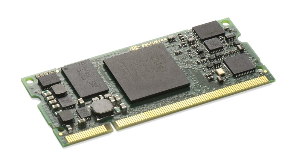 Enclustra's Mars ZX3 SOM Module
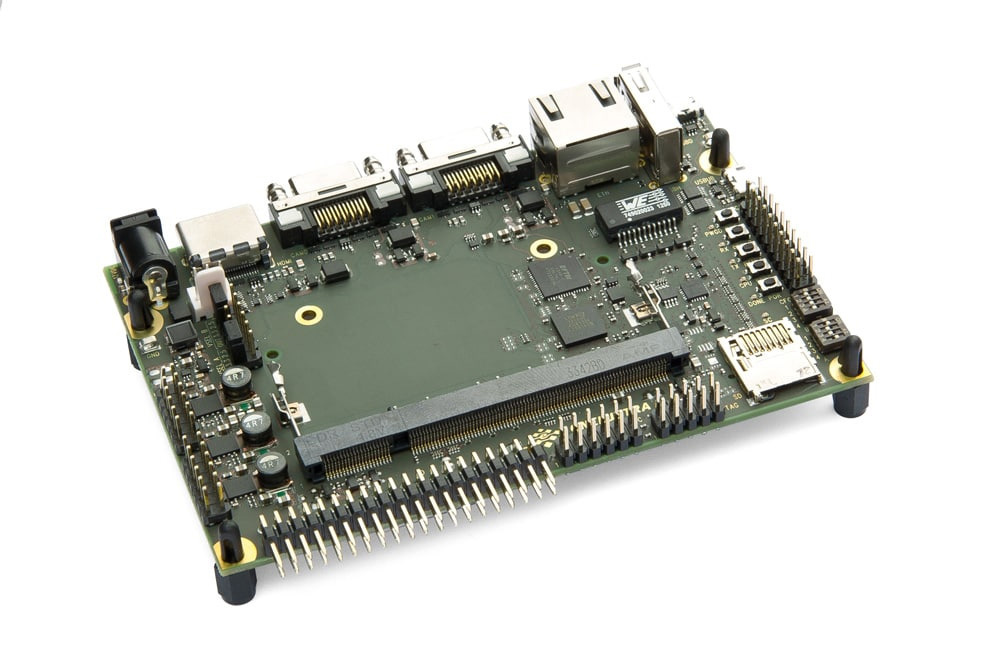 Enclustra's Mars EB1 Baseplate2. TI TLV320AIC34
 (
tlv320aic34evm-k and USB motherboard).
 Debug board for tlv320aic34 (tlv320aic34evm-k)
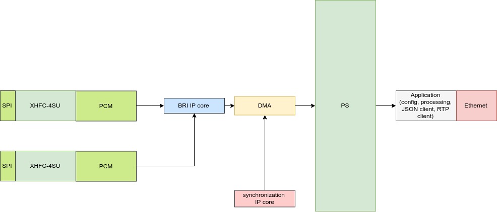
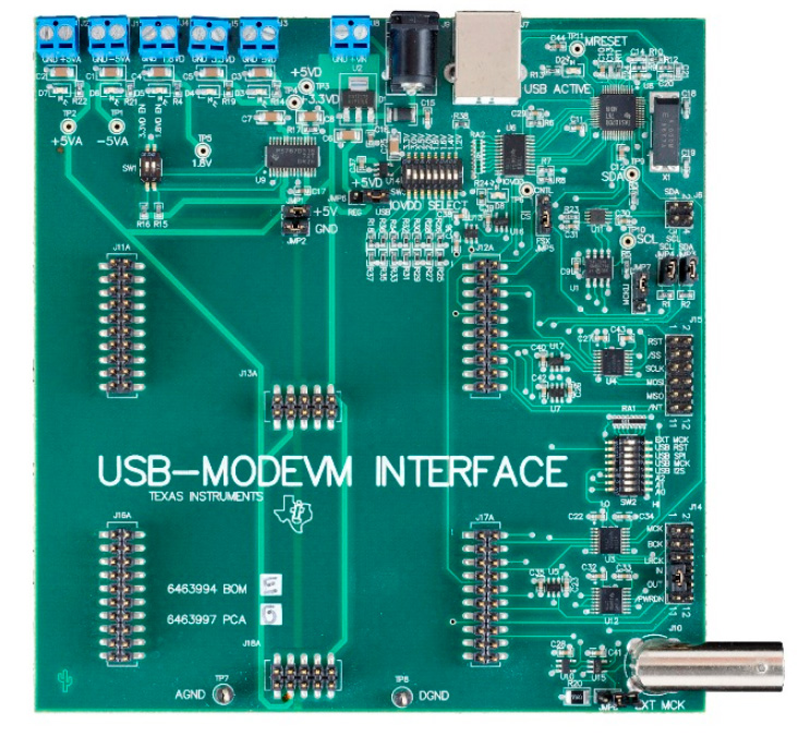 Expansion USB-MODEVM for tlv320aic34evm-k3. IDT82P2288 - PRI, XHFC-4SU - BRI chips,
 there were no debug kits, so we laid only the foundation as an ip-core for testing, and the baptism of fire took place right in the process, after making prototype boards.
Working with the system on a crystal Xilinx Zynq 7000
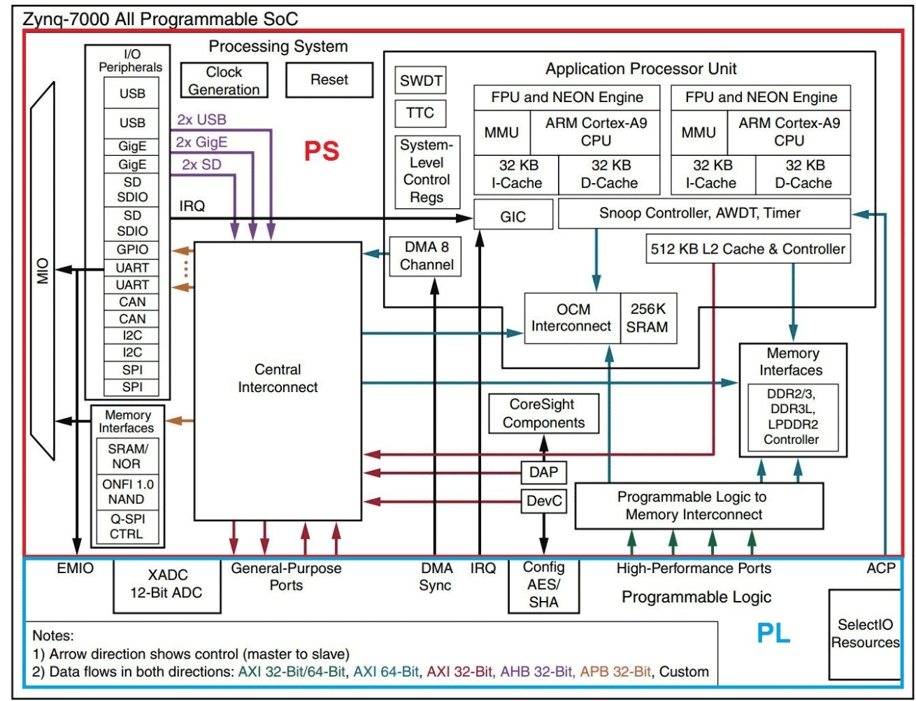 The internal structure of the SoC Xilinx Zynq 7000
 Steps for building boot files for Xilinx Zynq
The firmware / download of executable files for Zynq differs from the usual download for MPU. The usual work with Cortex-A processors is the u-boot, kernel linux, rootfs boot. And on Zynq appears bitstream, the firmware file for the FPGA (FPGA). Bitstream contains a description of hardware blocks on the FPGA and internal communication with the processor. This file is loaded at system startup. Also on the linux side there is a mechanism that allows flashing the PL-part immediately during operation, such a device is called xdevcfg (
ZYNQ FPGA manager since 2018.1 ).
PRI / BRI Interfaces
 Features of digital networks PRI / BRI
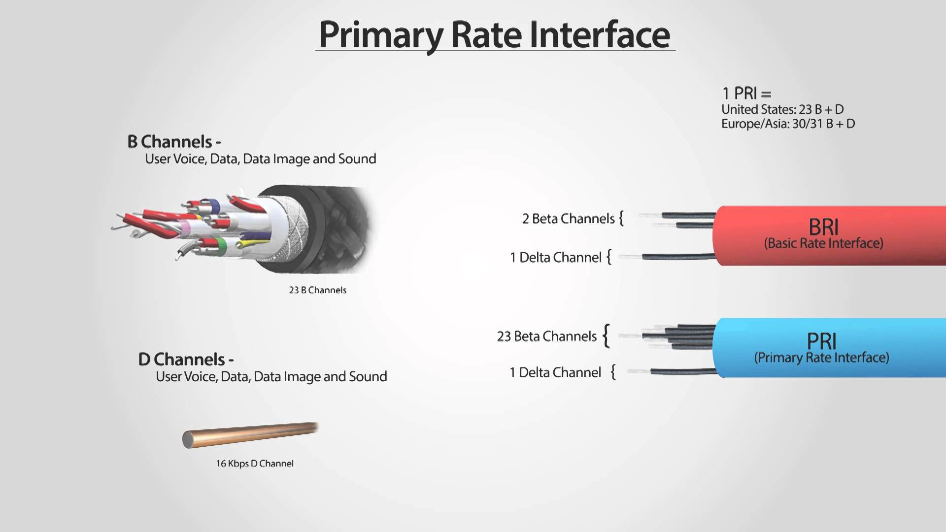
The Primary Rate Interface (PRI) is a standard ISDN network interface that defines the discipline for connecting ISDN stations to broadband backbones that connect local and central PBXs or network switches.
 Type of transmitted frame for PRI
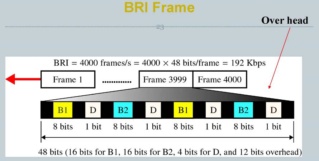 Transmission Frame Type for BRI
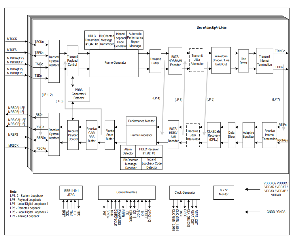 Internal Structure of PRI Physics - IDT82P2288
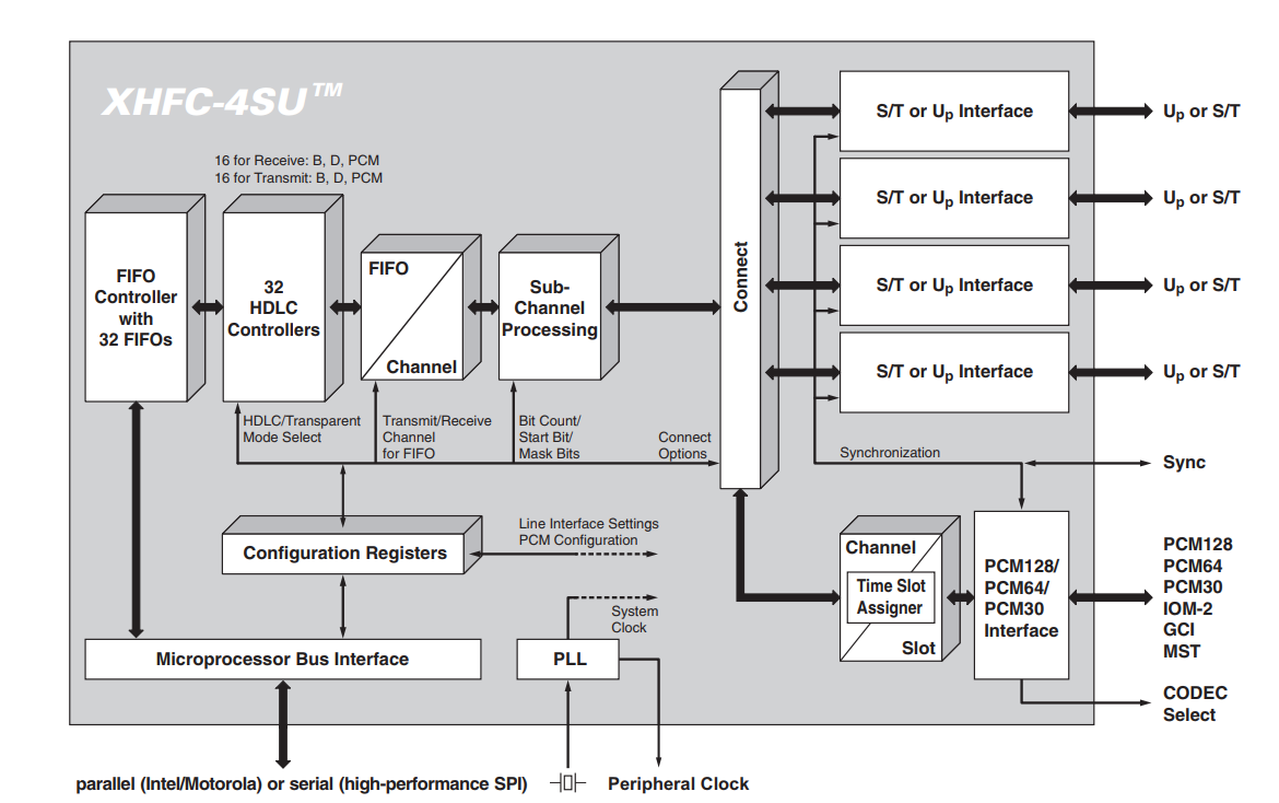 The internal structure of BRI physics - XHFC-4SU
Audio Codec TLV320AIC34
Four-channel low-power
audio codec TLV320AIC34 for portable audio and telephony is a good solution for use in analog telephony.
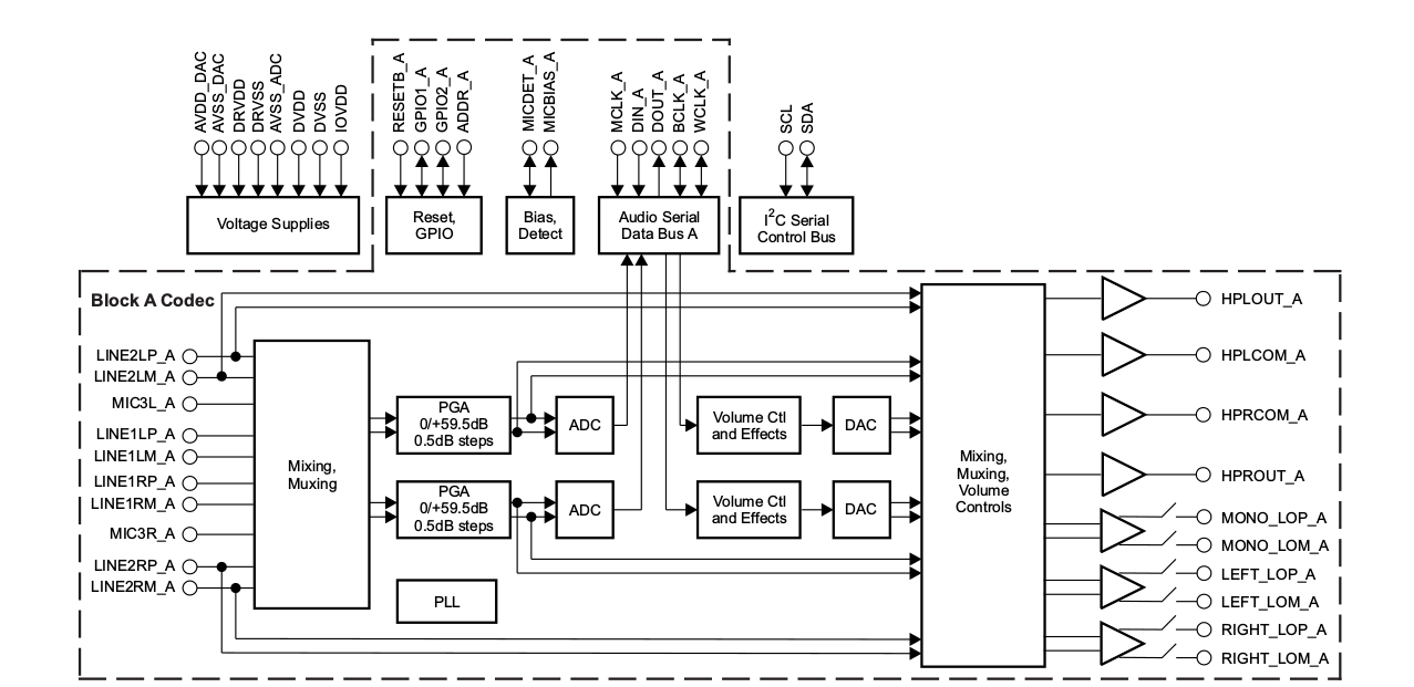 A-part tlv320aic34, audio codec contains two such functional blocks
Data can be transmitted via the I2S interface, as well as via DSP, PCM, TDM.
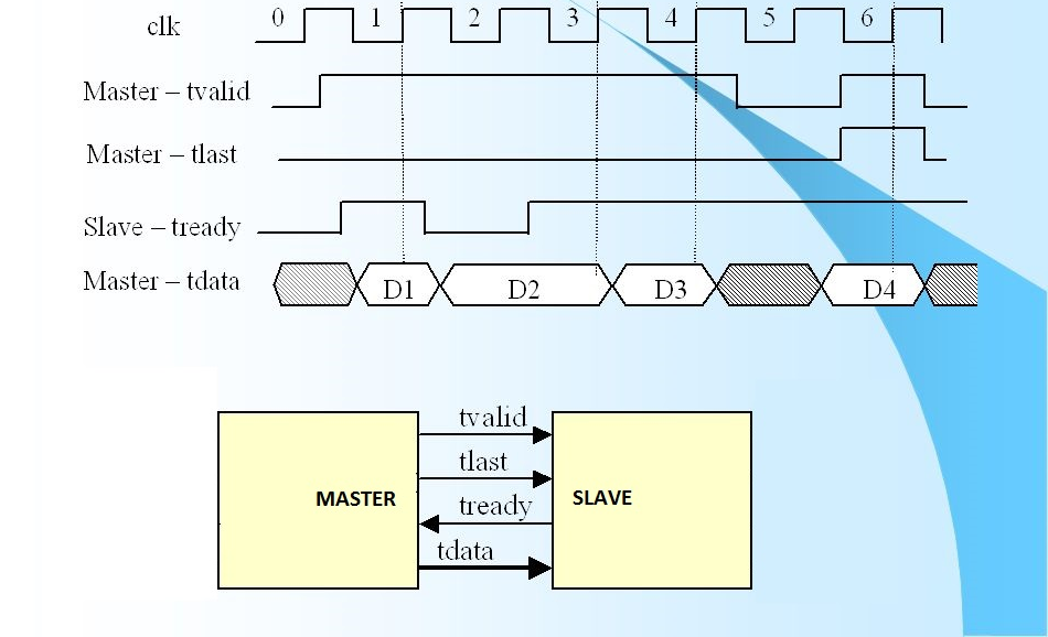
I2S is a serial bus interface standard, it is used to connect digital audio devices and electrically consists of 3 conductors that go from the active to the passive device, and 4 signals that correspond to them as follows:
- Bit Clock Clock (BCLK).
- Clock signal frame (according to) synchronization (WCLK).
- A data signal that can transmit or receive 2 time separated channels (DIN / DOUT).
The channels for receiving and transmitting data are separated, that is, there is a separate channel for receiving data and a channel for transmitting. The controller accepts data that the audio codec transmits, but the opposite is possible.
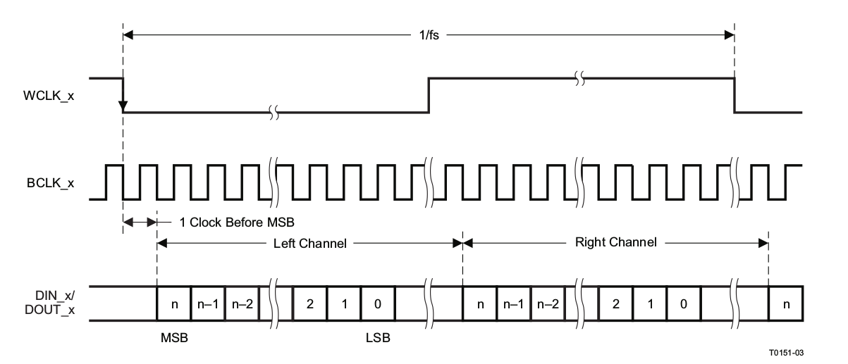 I2S-frame, features of the I2S-interface
After selecting all the hardware components, we solved the problem of connecting the audio codec and Xilinx Zynq 7020.
Search for I2S cores
Probably the most difficult moment when working with audio streams in the Xilinx Zynq 7020 was that, in principle, there is no I2S-bus on the chip in the system, so it was necessary to find the I2S-cores. This task was complicated by the condition that the ip-core had to be free.
We stopped at several ip-cores. Found for the bare metal core I2S
Digilent . Found several ip-cores on
opencores and, probably, the best option for us is the
Analog Devices ip-core. They produce ip-cores for their equipment, for FPGA / FPGA interaction.
We are interested in the ip-core called
AXI-I2S-ADI. The company itself Analog Devices promotes these ip-cores for their hardware platforms.
Total list of use cases for work:
- Bare metal - IP core for I2S (Digilent ZYBO audio)
- opencores.org
- AXI-I2S-ADI controller (Analog Devices)
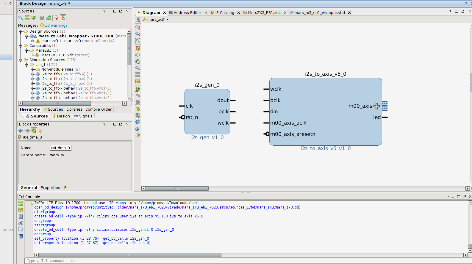
IP core AXI-I2S-ADI
The ip-core itself looks like this: it has the lines bclk, wclk, din, dout. It connects to the DMA Xilinx Zynq 7000; in our example, the DMA PS part is used. All data exchange takes place via DMA. DMA can be a separate unit or part of a PS SoC.
When configuring this ip-core, it is important not to forget to send the mclk master frequency to the tlv320aic34 itself, as an option when using the tlv320aic34 debug kit - to feed the external master frequency.
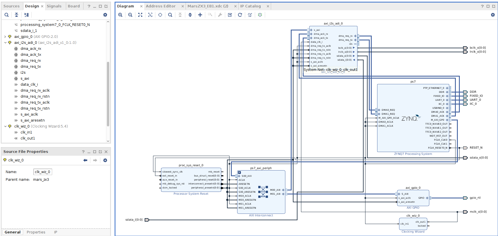 Function block with axi-i2s-adi connected
After the configuration procedure, the task was to launch the functionality in the Linux OS.
Starting and configuring the device tree for tlv320aic34
I2c configuration (tlv320aic34 is configured on this interface):
i2c0: i2c@e0004000 { ... tlv320aic3x: tlv320aic3x@18 { #sound-dai-cells = <0>; compatible = "ti,tlv320aic3x"; reg = <0x18>; gpio-reset = <&axi_gpio_0 0 0>; ai3x-gpio-func = <&axi_gpio_0 1 0>, /* AIC3X_GPIO1_FUNC_DISABLED */ <&axi_gpio_0 2 0>; /* AIC3X_GPIO2_FUNC_DIGITAL_MIC_INPUT */ AVDD-supply = <&vmmc2>; DRVDD-supply = <&vmmc2>; IOVDD-supply = <&vmmc2>; DVDD-supply = <&vmmc2>; ai3x-micbias-vg = <1>; }; ... };
I2s setup (audio data is transmitted via this interface):
i2s_clk: i2s_clk { #clock-cells = <0>; compatible = "fixed-clock"; clock-frequency = <11289600>; clock-output-names = "i2s_clk"; }; axi_i2s_adi_0: axi_i2s_adi@43C00000 { compatible = "adi,axi-i2s-1.00.a"; reg = <0x43C00000 0x1000>; xlnx,bclk-pol = <0x0>; xlnx,dma-type = <0x1>; xlnx,has-rx = <0x1>; xlnx,has-tx = <0x1>; xlnx,lrclk-pol = <0x0>; xlnx,num-ch = <0x1>; xlnx,s-axi-min-size = <0x000001FF>; xlnx,slot-width = <0x18>; }; &axi_i2s_adi_0 { #sound-dai-cells = <0>; compatible = "adi,axi-i2s-1.00.a"; clocks = <&clkc 15>, <&i2s_clk>; clock-names = "axi", "ref"; dmas = <&dmac_s 0 &dmac_s 1>; dma-names = "tx", "rx"; };
Sound card setup in device tree (audio card):
sound { compatible = "simple-audio-card"; simple-audio-card,name = "TLV320AIC34"; simple-audio-card,format = "i2s"; simple-audio-card,bitclock-master = <&dailink0_master>; simple-audio-card,frame-master = <&dailink0_master>; simple-audio-card,widgets = ... simple-audio-card,routing = ... dailink0_master: simple-audio-card,cpu { clocks = <&i2s_clk>; sound-dai = <&axi_i2s_adi_0>; }; simple-audio-card,codec { clocks = <&i2s_clk>; sound-dai = <&tlv320aic3x>; }; }; };
After all the manipulations to configure and configure the codec in the device tree in Linux, the cherished audio card appeared and we were able to hear the music (our first music track is Highway to Hell, AC / DC).
Here is what we had to do for this:
- Formed the necessary frequency using clk_wiz (clocking wizard)
- Properly configured DTS for tlv320aic34
- Added tlv320aic3x driver support
- Added audio packages to buildroot to play audio stream (aplay, madplay, etc.)
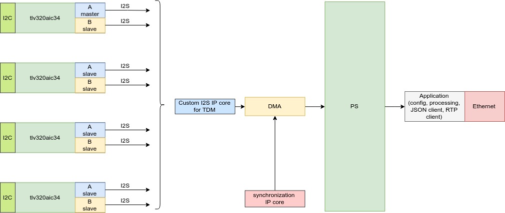
During the development of the final device, we faced the task of connecting 4 tlv320aic34 chips. The tlv320aic34 chip described above contains 2 blocks for working with audio streams, each block has its own i2c line for configuring and configuring audio parameters. A block can have only four addresses, respectively, it is impossible to connect four tlv320aic34 chips to one i2c interface, you need to use two i2c interfaces (8 independent audio blocks). For each block, if you start mclk, blck, wclk, din / dout individually, you need to add 40 signal lines in total, which is impossible and irrational from a circuit design point of view for the som module we have chosen, because besides these signals it was necessary to connect many other lines and interfaces.
As a result, we decided to switch the audio card to a
TDM mode , in which all mclk, bclk, din, dout lines are combined, which allows reducing the total number of communication lines. This decision influenced the work of axi-i2s-adi, due to the fact that the ip-core itself worked in master mode. Also, this change did not allow us to use our ip-core in TDM mode, and with a strong-willed decision we had to abandon the use of the selected ip-core. I had to write an ip-core to listen to i2s-traffic and send it to dma, this solution allowed us to create a common interface for receiving data that would not depend on the type of board for recording conversations (analog and digital boards).
The initial architecture of receiving an audio stream and processing it via the i2s interface:
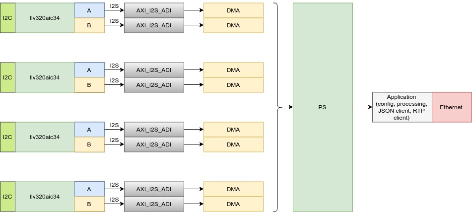
The final architecture for receiving an audio stream and processing it via an i2s interface:
Architecture of receiving a PRI stream and its processing:

Architecture of receiving a BRI stream and processing it:
AXI DMA
This is an important element of data synchronization for dma.
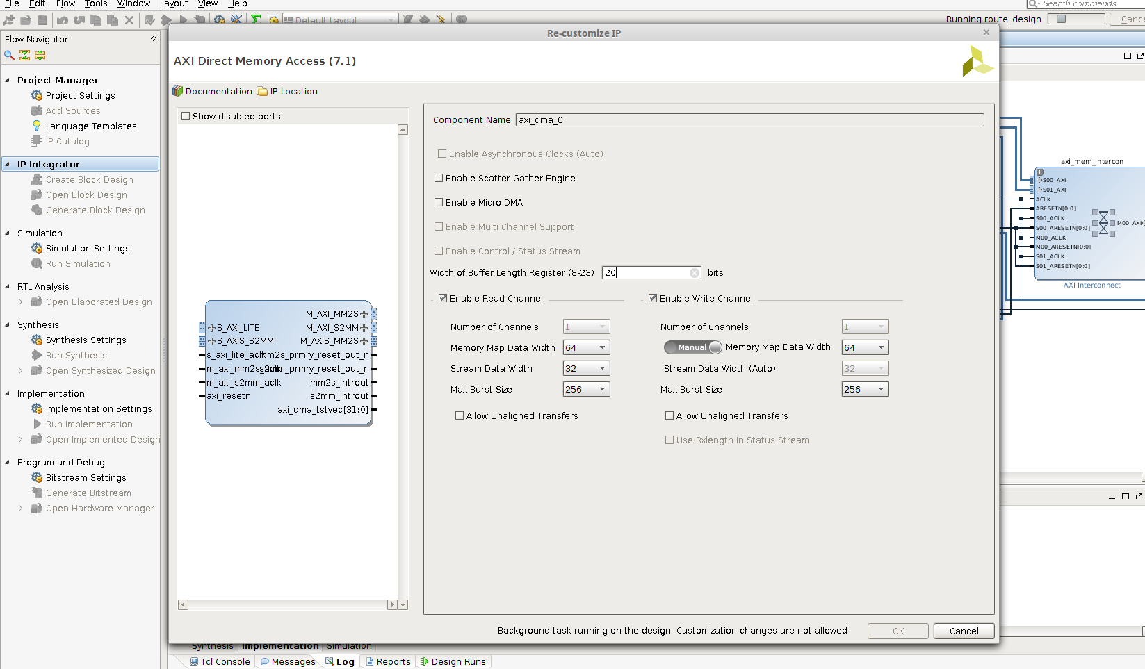 AXI DMA configuration window in Xilinx Vivado
The AXI DMA block itself is presented on the print screen. He has many options. You can configure the bus how much data to transmit. Data can be aligned or be in any format. A detailed description of the work and interaction with axi dma is described
in the technical documentation (version to version is the addition and correction of inaccuracies in the description, as well as the refinement of ip-cores).
AXI DMA Transmission Verification, AXI DMA Test Options
When developing the driver, we decided to find open source and adapt it to our task. In the end, we chose the source code of the
github-project ezdma (wordplay, read as easy dma).
The next step is the development of a test driver; this was the preparatory stage in anticipation of the moment when the ip-core comes to us with the ready-made functionality from the FPGA development department (the described development process was formed by the embedded programmers). Before this moment, we decided to take AXI DMA, AXI DATA FIFO and loop to insure against possible future errors. We looped the sending and receiving of data, so we checked the result of our work and the performance of our driver. We have slightly adapted the functionality, brought it to our wishes on the interaction interface and once again checked the performance of the driver and the chosen principle of interaction.
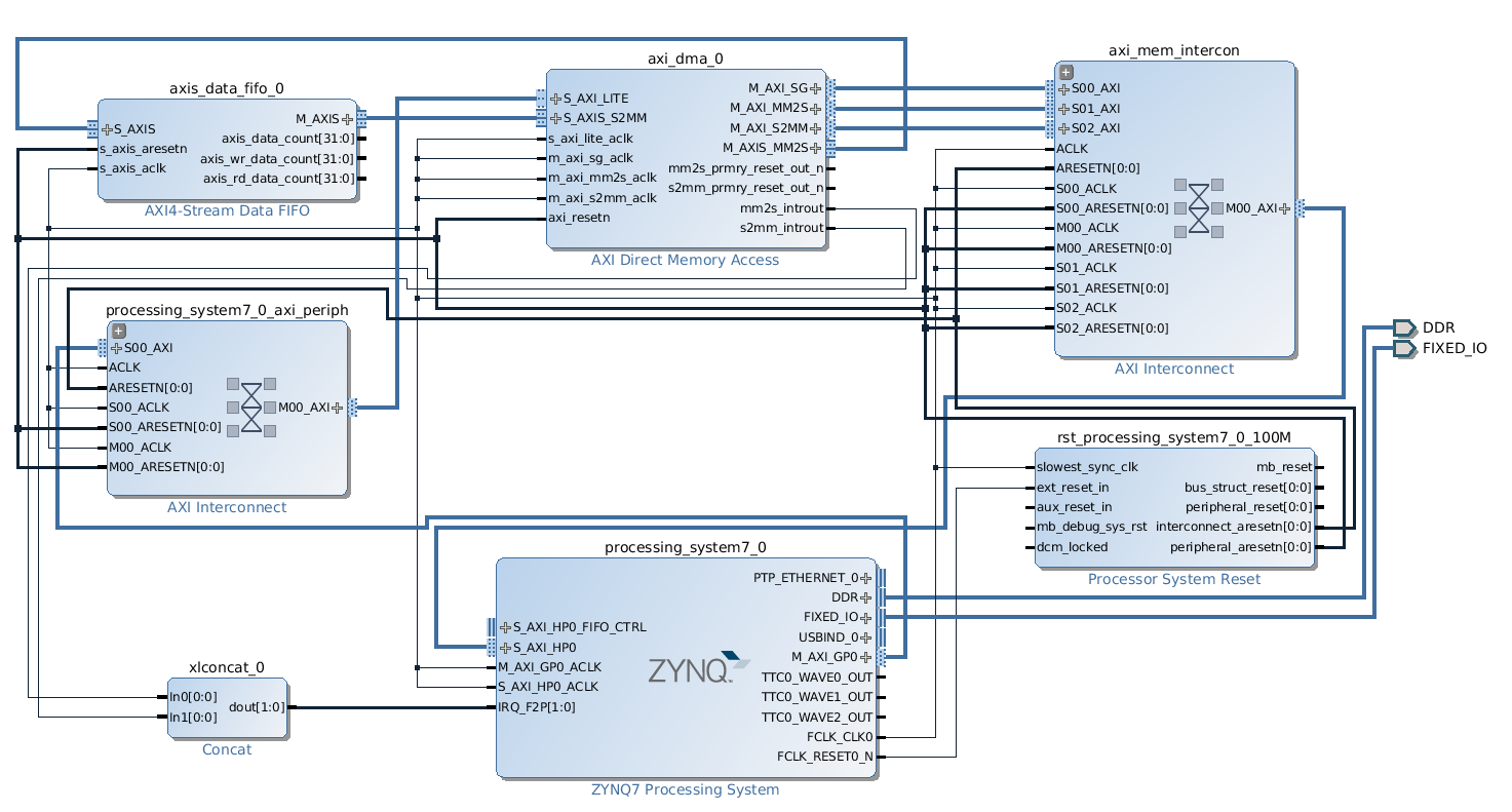 Look-back block design, the first way to check AXI DMA
Example description of DMA and ezdma in device tree:
/ { amba_pl: amba_pl { #address-cells = <1>; #size-cells = <1>; compatible = "simple-bus"; ranges ; axi_dma_1: axi_dma { #dma-cells = <1>; compatible = "xlnx,axi-dma-1.00.a"; reg = <0x40400000 0x10000>; clock-names = "s_axi_lite_aclk", "m_axi_sg_aclk", "m_axi_mm2s_aclk", "m_axi_s2mm_aclk"; clocks = <&clkc 15>, <&clkc 15>, <&clkc 15>, <&clkc 15>; interrupt-parent = <&intc>; interrupts = <0 29 4 0 30 4>; xlnx,addrwidth = <0x20>; xlnx,include-sg; dma-channel@40400000 { compatible = "xlnx,axi-dma-mm2s-channel"; dma-channels = <0x1>; interrupts = <0 29 4>; xlnx,datawidth = <0x20>; xlnx,device-id = <0x0>; xlnx,include-dre ; }; dma-channel@40400030 { compatible = "xlnx,axi-dma-s2mm-channel"; dma-channels = <0x1>; interrupts = <0 30 4>; xlnx,datawidth = <0x20>; xlnx,device-id = <0x0>; xlnx,include-dre ; }; }; ezdma0 { compatible = "ezdma"; dmas = <&axi_dma_1 0 &axi_dma_1 1>; dma-names = "loop_tx", "loop_rx"; // used when obtaining reference to above DMA core using dma_request_slave_channel() ezdma,dirs = <2 1>; // direction of DMA channel: 1 = RX (dev->cpu), 2 = TX (cpu->dev) }; ... }; };
Generating dts / dtsi files can be easily done using the
Device Tree Generator tool .
The second step in our development process is to create a test ip-core to test the driver, only this time the data will be meaningful, transferring to AXI_DMA via AXIS (as it will be in the final ip-core version).
 AXIS interface workflow
We implement two variants of ip-cores for data generation, the first proven option is the implementation through verilog, the second - on HLS (HLS in this context appeared under the slogan "stylishly-fashionable youth").
The data generator on verilog (and in general in the languages of the hdl-verilog, vhdl, etc.) family is a standard solution when developing this type of ip-cores. Here are short excerpts of intermediate ip-kernel code:
module GenCnt ( …. assign HandsHake = m_axis_din_tready & m_axis_dout_tvalid; always @(posedge Clk) begin if (Rst) begin smCnt <= sIDLE; end else begin case (smCnt) sIDLE: begin smCnt <= sDATA; end sDATA: begin if (Cnt == cTopCnt - 1) begin smCnt <= sLAST; end end ... endmodule
There is no need for a more detailed description, since this is a typical task for an FPGA designer.
More interesting "animal" here is HLS.
Vivado HLS (High Level Synthesis) is a new Xilinx CAD system for creating digital devices using high-level languages such as OpenCL, C or C ++.
C / C ++ is the main languages for the firmware engineer, so solving the problem using these languages is more interesting in terms of implementation and comparative analysis for future projects.
Let's give two small examples on working with HLS. The first example is the data generator for AXI_DMA, the second example is the data exchange between the processor part and the programmable logic via the s_axilite interface.
Data exchange via the s_axilite interface (second example) was implemented so that at any time in procfs one could deduct which bitstream is loaded, and so that one could track the correctness of work on versioning for the SoC PL part. A very interesting point appears here with s_axilite: Vivado HLS generates a driver for Linux (in turn, we adapted the driver to work through procfs in order to preserve the heredity of writing). The example generated code for Linux is below (the path to the source code is solution1 / impl / ip / drivers / name_xxx / src /).
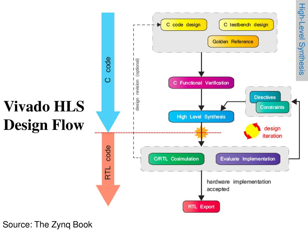 Stages of HLS synthesis and rtl code formation
Generator data on HLS to test the work with AXI_DMA:
#include <ap_axi_sdata.h> #include <hls_stream.h> #define SIZE_STREAM 1024 struct axis { int tdata; bool tlast; }; void data_generation(axis outStream[SIZE_STREAM]) { #pragma HLS INTERFACE axis port=outStream int i = 0; do{ outStream[i].tdata = i; outStream[i].tlast = (i == (SIZE_STREAM - 1)) ? 1 : 0; i++; }while( i < SIZE_STREAM); }
Example of getting the version and type of interface card:
#include <stdio.h> void info( int &aVersion, int &bSubVersion, int &cTypeBoard, int version, int subVersion, int typeBoard ){ #pragma HLS INTERFACE s_axilite port=aVersion #pragma HLS INTERFACE s_axilite port=bSubVersion #pragma HLS INTERFACE s_axilite port=cTypeBoard #pragma HLS INTERFACE ap_ctrl_none port=return aVersion = version; bSubVersion = subVersion; cTypeBoard = typeBoard; }
As you have noticed, it is very important to understand the work and application of various pragmas (HLS pragma) for developing on hls, since the synthesis process is directly tied to pragmas.
Generated s_axilite driver:
An important file that tells you the location of variables (registers) in the address space is x # your_name # _hw.h. You can always verify the correctness of the written ip-kernel using the devmem tool.
Contents of this file:
This file describes the addresses of registers, registers correspond to the location of arguments in the function. After the synthesis of the project, you can see how the created project will be performed in cycles.
 An example of the project execution by measure
Working with hls showed that this tool is suitable for quick solution of the tasks set, especially it has worked well for solving mathematical problems of computer vision, which can be easily described in C ++ or C, as well as for creating small ip-cores for interactions and exchanges information with standard FPGA interfaces.
In this case, HLS is not suitable for implementing specific hardware interfaces, for example, in our case it was I2S, and the generated rtl-code takes up more space on the FPGA than written in standard hdl-languages.
The last step in testing the driver is the development of the I2S traffic generator. This ip-core replicates the functionality of previous ip-cores, except for the fact that incremental data (traffic) is formed on it, which correspond to the real I2S data in TDM mode.
 Block design of future custom I2S-core testing and I2S traffic generator
As a result, we received the results of the work of hls, axi dma and s_axilite, checked the performance of our software and drivers.
findings
We managed to develop the necessary types of interface cards, as well as ip-cores for tdm, pri, bri. We have significantly improved the current approach in the development of such devices and created a comprehensive solution that can compete with similar interface cards from
Asterick ,
patton and others. The advantage of our solution is that the developer does not need an intermediate PC communication link with PCI for data transfer, he will be able to directly transmit the received information via Ethernet.