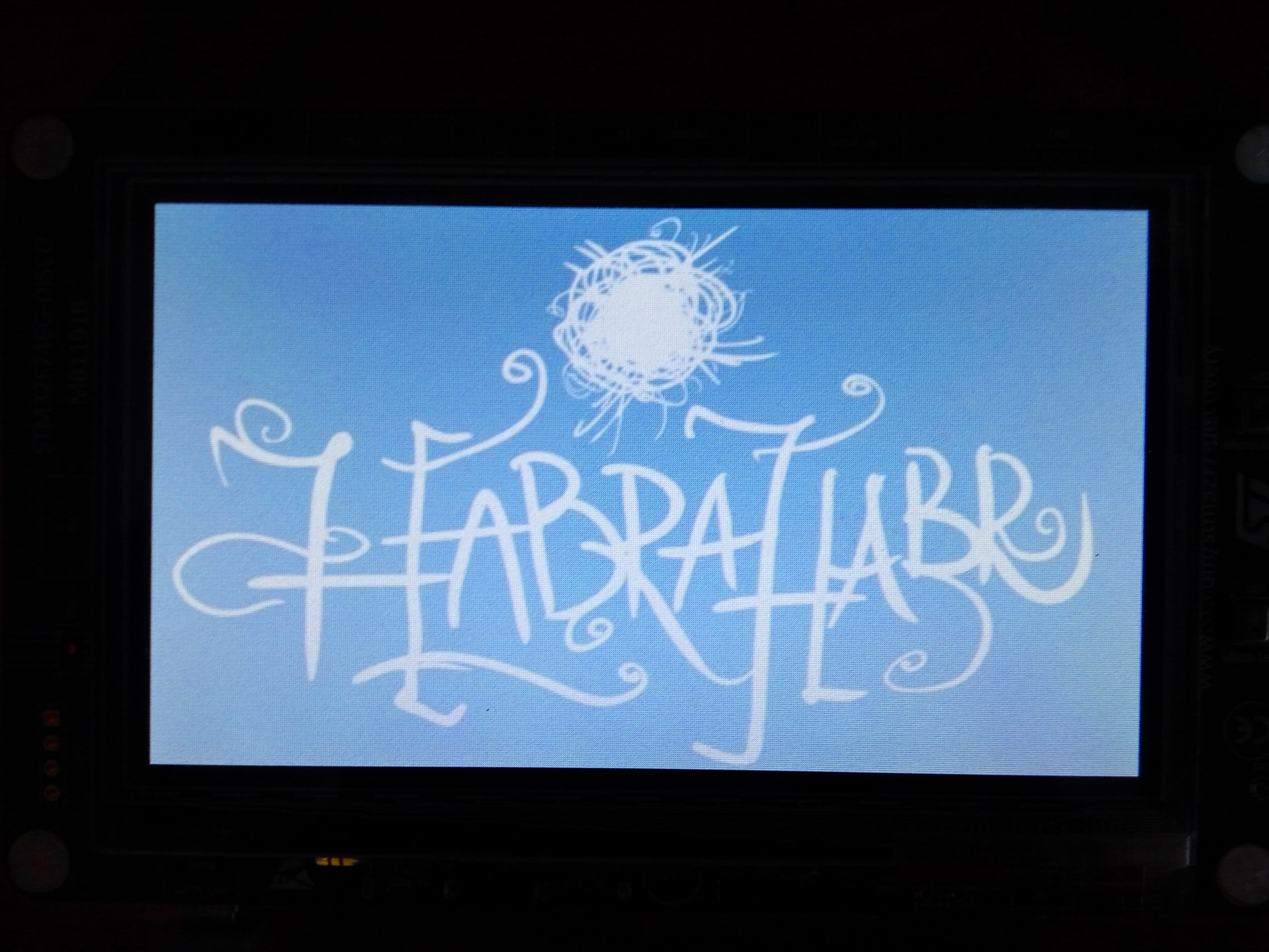
Greetings Recently, the project required to launch a display that had an LVDS interface. To implement the task, the STM32F746 controller was chosen, since I have already worked with him quite a lot and he has a LTDC module that allows you to work directly with the display without a controller. In this case, the controller is already implemented inside the microcontroller. It was also not the last argument that the STM32F746-Disco was on this stone, which I had at hand, which means I could start working on the project without waiting for me to pay for the board, components, and so on.
Today I will tell you how to run the LTDC module, working with registers (CMSIS). HAL and other libraries do not like and do not use for religious convictions, but this is also an interest. You will see that raising complex peripherals on registers is as easy as regular SPI. Interesting? Then let's go!
1. A little about LTDC
This peripheral module is essentially a controller that usually stands on the display side, for example, SSD1963 and similar ones. If we look at the LTDC structure, we will see that physically it is a parallel 24-bit bus + hardware graphics accelerator + data array in RAM, which is in fact a display buffer (frame buffer).
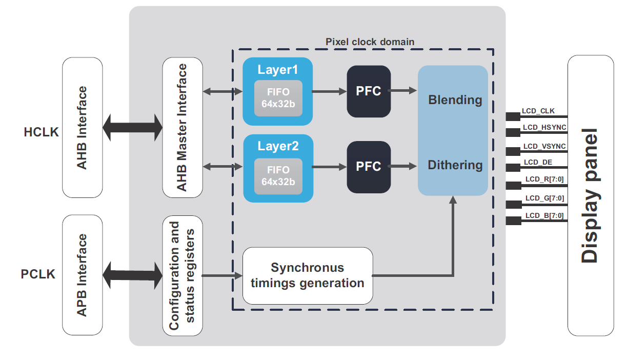
At the output, we have a regular parallel bus, which contains 24 bits of color (8 bits per color of the RGB model), clock lines, display on / off lines and pixel clock. The latter is in fact a clock signal for which pixels are loaded into the display, that is, if we have a frequency of 9.5 MHz, then in 1 second we can load 9.5 million pixels. It is in theory, of course, in practice the numbers are somewhat more modest due to timings and other things.
For more information about LTDC, I advise you to read a few documents:- Overview of LTDC capabilities in F4, in our F7 all the same
- Application note 4861. "LCD-TFT display controller (LTDC) on STM32 MCUs"
2. What do we need to do?
Microcontrollers from ST have gained popularity for good reason, the most important requirement for any electronic components is documentation, and everything is fine with it. The site is terrible, of course, but I’ll leave links to all the documentation. The manufacturer saves us from the torment and invention of the bicycle, so on page 520 in the
reference manual RM0385 black and white is
described in steps, what we need to do:
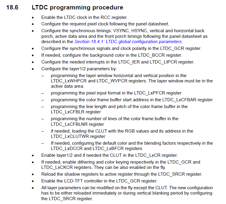
In fact, half of this will not have to be done: it is either not needed to start, or it is already configured by default. For the minimum start, which will allow us to draw pixels, display images, graphics, text, etc., it’s enough to do the following:
- Enable clocking of LTDC module
- Configure the clocking system and the frequency of data output (pixel clock)
- Configure I / O ports (GPIO) to work with LTDC
- Set up timings for our display model.
Adjust the polarity of the signals. Already done by defaultSpecify the background color of the display. We will not see it yet, you can leave it "by zeros"- Set the actual size of the visible display area for a specific layer
- Select a color format: ARGB8888, RGB 888, RGB565, etc.
- Specify the address of the array, which will act as a frame buffer
- Specify the amount of data in one line (length by width)
- Specify the number of lines (display height)
- Include layer we work with
- Enable LTDC Module
Fearfully? And I was scared, and there it turned out work for 20 minutes with all the proceedings. The task is, the plan is painted and it remains only to complete it.
3. Setting up the clocking system
The first item we need to send a clock signal to the LTDC module, this is done by writing to the RCC register:
RCC->APB2ENR |= RCC_APB2ENR_LTDCEN;
Next, you need to adjust the clocking frequency from external quartz (HSE) to 216 MHz, that is, to the maximum. The first step is to turn on the clock source from the quartz resonator and wait for the ready flag:
RCC->CR |= RCC_CR_HSEON; while (!(RCC->CR & RCC_CR_HSERDY));
Now we set the delay for the controller's flash memory, since She does not know how to work on the core frequency. Its value as the rest of the data is taken from the reference manual:
FLASH->ACR |= FLASH_ACR_LATENCY_5WS;
Now, to get the desired frequency, I will divide 25 MHz from the input by 25 and get 1 MHz. Further, just in PLL I multiply by 432, since In the future, there is a frequency divider with a minimum value of / 2 and you need to apply a double frequency to it. After that, we connect the PLL input to our quartz resonator (HSE):
RCC->PLLCFGR |= RCC_PLLCFGR_PLLM_0 | RCC_PLLCFGR_PLLM_3 | RCC_PLLCFGR_PLLM_4; RCC->PLLCFGR |= RCC_PLLCFGR_PLLN_4 | RCC_PLLCFGR_PLLN_5 | RCC_PLLCFGR_PLLN_7 | RCC_PLLCFGR_PLLN_8; RCC->PLLCFGR |= RCC_PLLCFGR_PLLSRC;
Now turn on the PLL and wait for the ready flag:
RCC->CR |= RCC_CR_PLLON; while((RCC->CR & RCC_CR_PLLRDY) == 0){}
We assign the output of our PLL as the source of the system frequency and wait for the ready flag:
RCC->CFGR |= RCC_CFGR_SW_PLL; while((RCC->CFGR & RCC_CFGR_SWS) != RCC_CFGR_SWS_1) {}
This is where the total clocking setting ends and we proceed to adjusting the clock frequency (PLLSAI) for our display (pixel clock). The signal for PLLSAI according to datasheet is taken after the divider / 25, that is, at the input we have 1 MHz. We need to get a frequency of about 9.5 MHz, for this the frequency of 1 MHz is multiplied by 192, and then with the help of two dividers by 5 and 4 we get the desired value PLLSAI = 1 MHz * 192/5/4 = 9.6 MHz:
RCC->PLLSAICFGR |= RCC_PLLSAICFGR_PLLSAIN_6 | RCC_PLLSAICFGR_PLLSAIN_7; RCC->PLLSAICFGR |= RCC_PLLSAICFGR_PLLSAIR_0 | RCC_PLLSAICFGR_PLLSAIR_2; RCC->DCKCFGR1 |= RCC_DCKCFGR1_PLLSAIDIVR_0; RCC->DCKCFGR1 &= ~RCC_DCKCFGR1_PLLSAIDIVR_1;
The final step is to enable PLLSAI for the display and wait for the ready flag:
RCC->CR |= RCC_CR_PLLSAION; while ((RCC->CR & RCC_CR_PLLSAIRDY) == 0) {}
This is the basic configuration of the clocking system completed, the only thing not to forget and then not to suffer, let's turn on clocking on all input / output ports (GPIO). The power supply is not battery-like at least on debugging, so we do not save:
RCC->AHB1ENR |= RCC_AHB1ENR_GPIOAEN; RCC->AHB1ENR |= RCC_AHB1ENR_GPIOBEN; RCC->AHB1ENR |= RCC_AHB1ENR_GPIOCEN; RCC->AHB1ENR |= RCC_AHB1ENR_GPIODEN; RCC->AHB1ENR |= RCC_AHB1ENR_GPIOEEN; RCC->AHB1ENR |= RCC_AHB1ENR_GPIOFEN; RCC->AHB1ENR |= RCC_AHB1ENR_GPIOGEN; RCC->AHB1ENR |= RCC_AHB1ENR_GPIOHEN; RCC->AHB1ENR |= RCC_AHB1ENR_GPIOJEN; RCC->AHB1ENR |= RCC_AHB1ENR_GPIOKEN;
4. Configure I / O ports (GPIO)
With gpio tuning, everything is very simple - we all have LTDC bus legs to be configured as an alternative output and at a high frequency. To do this, in the reference manual on page 201 we have the following hint:
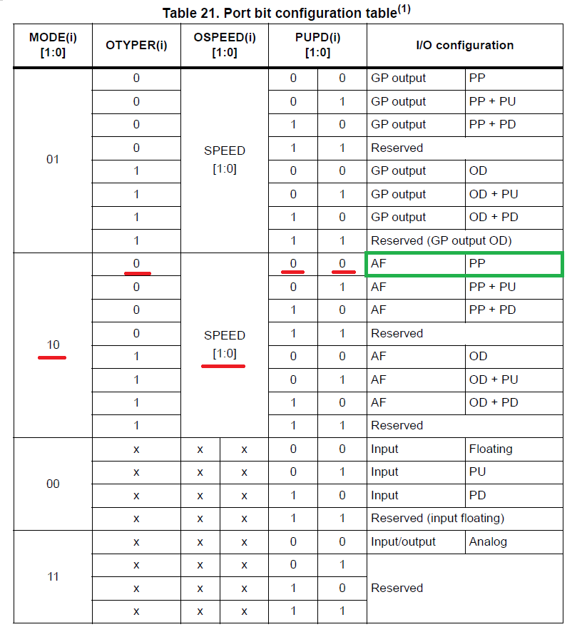
The table indicates which bits in the registers must be set in order to obtain the necessary setting. It is worth noting that all our suspenders are disabled. Where to see which alternative function to include? And for this we go to page 76 in the
datasheet at our controller and look at the following table:
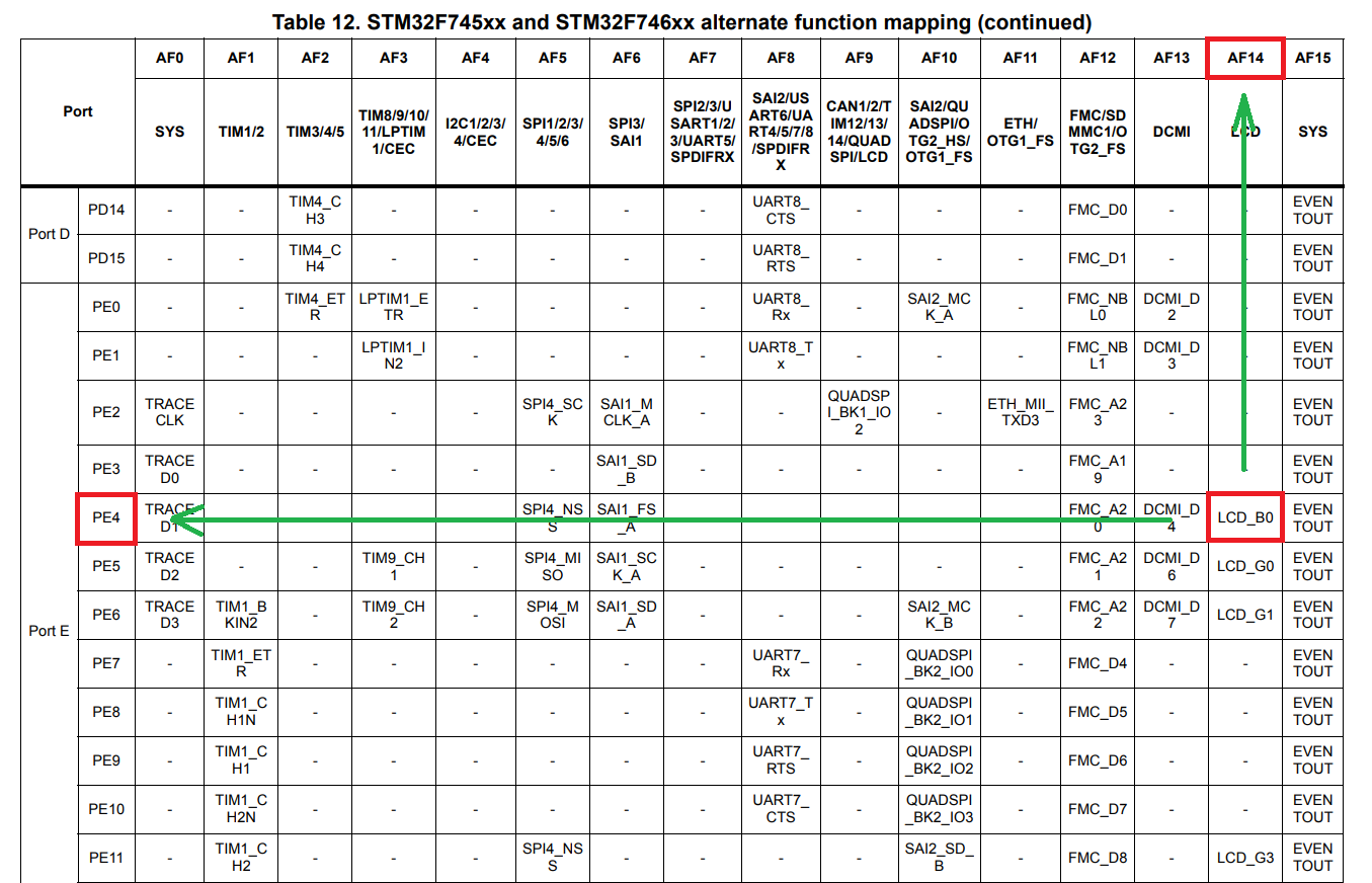
As you can see, the table logic is the simplest: we find the function we need, in our case LTDC B0, then we look at what GPIO it is (PE4, for example) and at the top we look at the number of the alternative function that we will use to configure (AF14 with us). To configure our output as a push-pull output with an alternative function LTDC B0, we need to write the following code:
GPIOE->MODER &= ~GPIO_MODER_MODER4; GPIOE->MODER |= GPIO_MODER_MODER4_1; GPIOE->OSPEEDR |= GPIO_OSPEEDER_OSPEEDR4_1; GPIOE->AFR[0] &= ~GPIO_AFRL_AFRL4_0; GPIOE->AFR[0] |= GPIO_AFRL_AFRL4_1 | GPIO_AFRL_AFRL4_2 | GPIO_AFRL_AFRL4_3;
I gave an example for PE4 output, which corresponds to the output B0 on the LTDC bus, that is, it is the zero bit of blue. For all other outputs, the setting is identical, only 2 outputs deserve special attention, one of the ready ones includes the display, and the other one is illuminated. They are configured as a normal push-pull output, which everyone uses to flash the LED. The setting looks like this:
GPIOK->MODER &= ~GPIO_MODER_MODER3; GPIOK->MODER |= GPIO_MODER_MODER3_0;
This setting is for PK3 output, which turns our backlight on and off. By the way, it is also possible to PWM to smoothly adjust the brightness. For PI12, which includes a display (DISP), everything is the same. The speed on these 2 pins is low by default, because some high-frequency actions are not required from them.
You can look at all the other I / O ports by yourself on the debugging circuit board, or on the circuit diagram of your own device.
5. Timings and their settings
Timings from a physical point of view are normal delays. I think you have repeatedly observed various distortions like delay (1), when you looked at code examples on displays with SPI / I2C controllers like ILI9341. There, a delay is needed in order for the controller, for example, to manage to accept a command, execute it, and then do something with the data. In the case of LTDC, everything is about the same, only we will not cram down crutches and why not - our microcontroller is able to form the necessary timings by hardware. Why are they needed on the display, where there is no controller? Yes, it's elementary to, after filling the first line of pixels, go to the next line and return to its beginning. This is due to the production technology of displays, and therefore each particular display model can have its own timings.
To find out what values we need, go to the ST site and look at
the STM32F746-Disco debug card . There we can see that the display is
RK043FN48H-CT672B and the documentation for it is available, for example,
here . We are most interested in the table on page 13 in section 7.3.1:
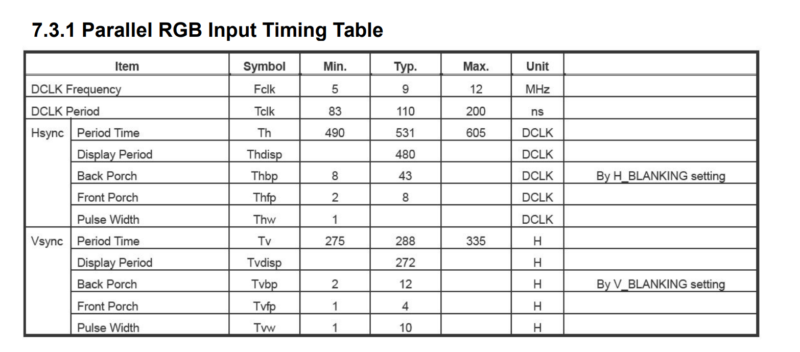
Here they are our values that we need when setting up. Also in the documentation there are a lot of interesting things, for example, diagrams of signals on the bus, etc., which you may need if, for example, you want to raise the display to FPGA or CPLD.
Go to the settings. First of all, in order not to keep these values in my head, I will draw them in the form of defines:
#define DISPLAY_HSYNC ((uint16_t)30) #define DISPLAY_HBP ((uint16_t)13) #define DISPLAY_HFP ((uint16_t)32) #define DISPLAY_VSYNC ((uint16_t)10) #define DISPLAY_VBP ((uint16_t)2) #define DISPLAY_VFP ((uint16_t)2)
There is an interesting feature. Timing
Pulse Width , which we
call DISPLAY_HSYNC , has a value in the table only for the pixel clock frequency of 5 MHz, and for 9 and 12 MHz it is not. This timing needs to be selected for your display, I got this value 30, when in the examples from ST it was different. When you first start if you have an error with its setting, the image will be shifted either to the left or to the right. If to the right - we decrease the timing, if to the left - we increase. In fact, it affects the beginning of the coordinates of the visible zone, which we will see further. Just keep in mind, and the following image from page 24 of our AN4861 will help you to comprehend the whole paragraph:
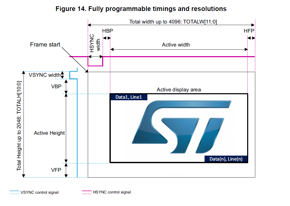
Here a small abstraction is convenient. We have 2 display zones: visible and common. The visible zone has dimensions with the declared resolution of 480 by 272 pixels, and the common zone is visible + our timings, which are 3 on each side. It is also worth understanding (this is no longer an abstraction) that one system tick is 1 pixel, so the total area has a size of 480 pixels + HSYNC + HBP + HFP.
It is also worth realizing that the lower the timings, the better - the display will be updated faster and the frame rate will increase slightly. Therefore, after the first start, experiment with the timings and reduce them as much as possible while maintaining stability.
To set up the timings, I have made myself a small “cheat sheet” inside the project for the future, it will also help you understand what specific number and where to enter it:
Where did this “crib” actually come from ... First, a similar “formula” you saw a couple of paragraphs before. Second, go to page 56 of our AN4861:
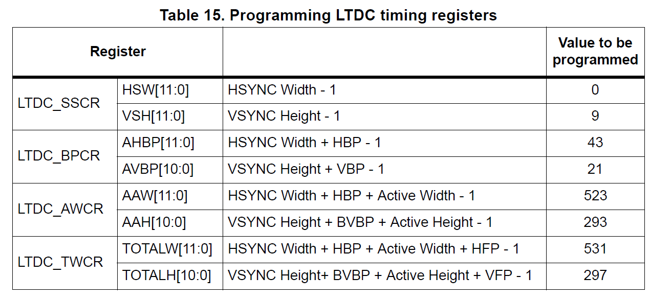
True, I hope that you understand the physical meaning of the timings even before the appearance of this cheat sheet and I am sure that you could surely make it yourself. There is nothing difficult in it, and the pictures from RM and AN help to visually understand the effect of timings on the image formation process.
Now it's time to write the code that will set up these timings. In the "cheat sheet" are specified the bits of the register in which to write, for example, TOTALH and after the sign is the formula giving the output a certain number. Clear? Then we write:
LTDC->SSCR |= ((DISPLAY_HSYNC - 1) << 16 | (DISPLAY_VSYNC - 1)); LTDC->BPCR |= ((DISPLAY_HSYNC+DISPLAY_HBP-1) << 16 | (DISPLAY_VSYNC+DISPLAY_VBP-1)); LTDC->AWCR |= ((DISPLAY_WIDTH + DISPLAY_HSYNC + DISPLAY_HBP - 1) << 16 | (DISPLAY_HEIGHT + DISPLAY_VSYNC + DISPLAY_VBP - 1)); LTDC->TWCR |= ((DISPLAY_WIDTH + DISPLAY_HSYNC + DISPLAY_HBP + DISPLAY_HFP -1)<< 16 |(DISPLAY_HEIGHT + DISPLAY_VSYNC + DISPLAY_VBP + DISPLAY_VFP - 1));
And on this with all the timings! In this section, you can even adjust the background color. I have it by default black, so written in zero. If you want to change the color of the background layer (background), then you can write down any value, for example,
0xFFFFFFFF and fill it with white:
LTDC->BCCR = 0;
There is a wonderful illustration in the
reference manual , which clearly demonstrates that we actually have 3 layers: background, layer 1 and layer 2. The background layer is “neutered” and can only be filled with one specific color, but it can also be incredibly useful when implementing future GUI design. Also, this illustration clearly demonstrates the priority of layers, from which it follows that we will see the fill color on the background only when the other layers are either empty or transparent.
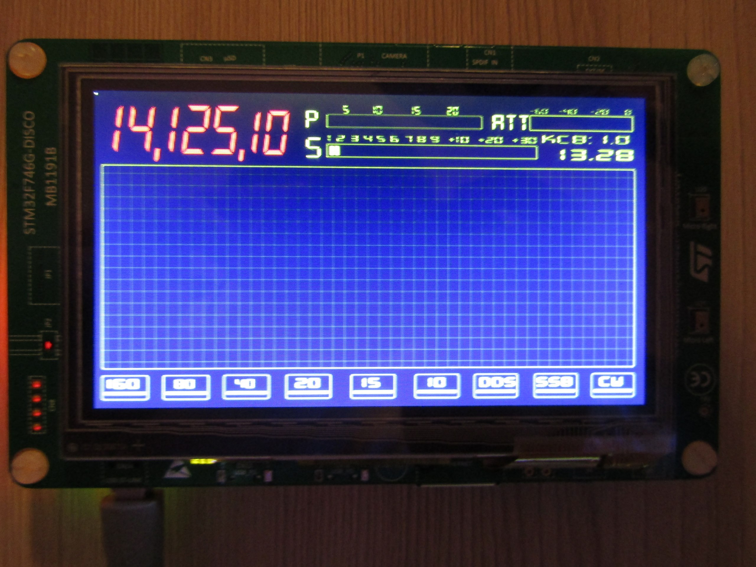
As an example, I will show one of the project pages, where during the implementation of the background template, one color was filled in and the controller redrawn not the whole page, but only individual sectors, which allowed to get about 50-60 fps for many other tasks:
6. The final part of the LTDC setup
LTDC settings are divided into 2 sections: the first are common for the whole LTDC module and are in the
LTDC register
group , and the second are configured in one of two layers and are in the
LTDC_Layer1 and
LTDC_Layer2 group .
We made the general settings in the previous paragraph, these include setting the timings of the background layer. Now we are going to adjust the layers and, according to our list, we need the real size of the visible zone of the layer, which is described in the form of 4 coordinates (x0, y0, x1, y2), allowing us to get the dimensions of the rectangle. The size of the visible layer may be less than the resolution of the display, no one bothers to make a layer size of 100 by 100 pixels. To adjust the size of the visible zone, we write the following code:
LTDC_Layer2->WHPCR |= (((DISPLAY_WIDTH + DISPLAY_HBP + DISPLAY_HSYNC - 1) << 16) | (DISPLAY_HBP + DISPLAY_HSYNC)); LTDC_Layer2->WVPCR |= (((DISPLAY_HEIGHT + DISPLAY_VSYNC + DISPLAY_VBP - 1) << 16) |(DISPLAY_VSYNC + DISPLAY_VBP));
As you can see, everything is just like with the timings. The starting points (x0, y0) of the visible zone consist of the sum of two timings: HSYNC + HBP and VSYNC + VBP. To calculate the coordinates of the end point (x1, y1), the width and height in pixels are simply added to the value data.
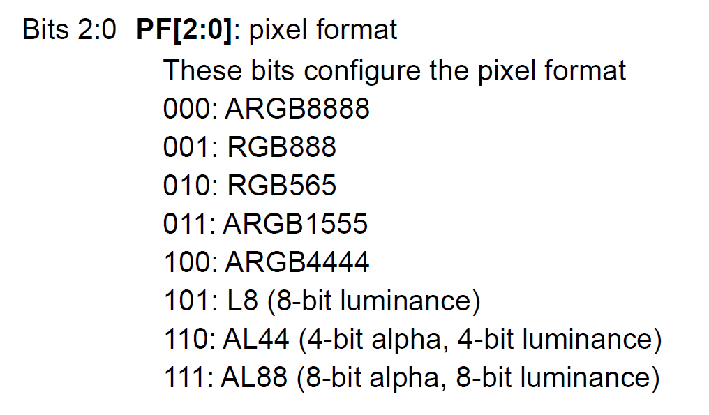
Now you need to configure the format of the received data. The maximum quality is obtained when using the ARGB8888 format, but at the same time we get the maximum amount of memory used. One pixel occupies 32 bits or 4 bytes, which means the entire screen takes 4 * 480 * 272 = 522,240 bytes, that is, half of the flash memory of our not very weak controller. You should not be afraid - the connection of external SDRAM and Flash memory via QSPI solves memory problems and there are no restrictions on this format, we rejoice at the good quality. If you want to save space or your display does not support 24-bit format, then more suitable models are used for this, for example, RGB565. A very popular format for both displays and cameras, and most importantly when using it, 1 pixel occupies only 5 + 6 + 5 = 16 bits or 2 bytes. Accordingly, the amount of memory occupied by the layer will be 2 times less. By default, the controller has already configured the ARGB8888 format and looks like this:
LTDC_Layer2->PFCR = 0;
If you need a different format other than ARGB8888, then go to pages 533 and 534 in the
reference manual and choose the desired format from the list provided:
Now we will create an array and pass its address to LTDC, it will turn into frame buffer and will be a "reflection" of our layer. For example, you need to fill the 1st pixel in the 1st line with white color, for this you just have to write the color value (0xFFFFFFFF) in the first element of this array. Need to fill the 1st pixel in the 2nd line? Then write the same color value into the element with the number (480 + 1). 480 - will make a line break, then add the number in the line we need.
This setting looks like this:
#define DISPLAY_WIDTH ((uint16_t)480) #define DISPLAY_HEIGHT ((uint16_t)272) const uint32_t imageLayer2[DISPLAY_WIDTH * DISPLAY_HEIGHT]; LTDC_Layer2->CFBAR = (uint32_t)imageLayer2;
For good, you should, after setting up LTDC, also configure SDRAM to remove the
const modifier and get the frame buffer in RAM, since own RAM MK is not enough even for one layer with 4 bytes. Although this does not hurt to test the correct configuration of the periphery.
Next, you need to specify the value of the alpha layer, that is, the transparency for our
Layer2 layer, for this we write the value from 0 to 255, where 0 is a fully transparent layer, 255 is completely opaque, that is, 100% visible:
LTDC_Layer2->CACR = 255;
According to our plan, it is now necessary to record the size of our visible display area in bytes, for this we write the corresponding values into the registers:
LTDC_Layer2->CFBLR |= (((PIXEL_SIZE * DISPLAY_WIDTH) << 16) | (PIXEL_SIZE * DISPLAY_WIDTH + 3)); LTDC_Layer2->CFBLNR |= DISPLAY_HEIGHT;
The last two steps remain, namely the inclusion of layer No. 2 and the LTDC periphery module itself. To do this, write the corresponding bits:
LTDC_Layer2->CR |= LTDC_LxCR_LEN; LTDC->GCR |= LTDC_GCR_LTDCEN;
At this, the setting of our module is finished and you can work with our display!
7. A little about working with LTDC
All work with the display is now reduced only to writing data to the
imageLayer2 array, it has a size of 480 by 272 elements, which fully corresponds to our resolution and hints at a simple truth -
1 array element = 1 pixel on the display .
As an example, I wrote a picture into an array, which I converted to in the
LCD Image Converter program, but in reality it is unlikely that your tasks will be limited to this. There are two ways: using the finished GUI and writing it yourself. For relatively simple tasks like text output, graphing and the like I advise you to write your GUI, it will take a little time and give you a complete understanding of its work. When the task is large and complex, and there is no time to develop your GUI, I advise you to pay attention to ready-made solutions, for example, uGFX and the like.
Text symbols, lines and other elements are inherently arrays of pixels, respectively, to implement them you need to implement logic yourself, but you should start with the most basic function - “pixel output”. It must take 3 arguments: the X coordinate, the Y coordinate and, accordingly, the color at which this pixel is colored. It may look like this:
typedef enum ColorDisplay { RED = 0xFFFF0000, GREEN = 0xFF00FF00, BLUE = 0xFF0000FF, BLACK = 0xFF000000, WHITE = 0xFFFFFFFF } Color; void SetPixel (uint16_t setX, uint16_t setY, Color Color) { uint32_t numBuffer = ((setY - 1) * DISPLAY_WIDTH) + setX; imageLayer2[numBuffer] = Color; }
After we have taken the coordinates to the function, we recalculate them into the number of the array that corresponds to the given coordinate, and then we write the received color to the received element. Based on this function, you can further implement the output functions of geometry, text, and other GUI “buns”. I think the idea is clear, but how to put it into practice is at your discretion.
Total
As you can see, the implementation of even complex periphery on registers (CMSIS) is not a difficult task, you just have to understand how it works inside. Of course, today it is fashionable to develop firmware without an understanding of what is happening, but this is a dead-end path if you plan to become an engineer, and not ...
If you compare the received code with the solution on HAL or SPL, then you will notice that the code written in registers is more compact. By adding where you need a couple of comments and wrapping up in a function, we get readability at least as good as HAL / SPL, and if we remember that the
reference manual documents the registers, then working with CMSIS is more convenient.
1) The source project in TrueSTUDIO can be downloaded
here.2) For those who are more comfortable to look at
GitHub3) The utility for converting images into code LCD Image Converter download
here