 Part IPart IIPart IIIPart IVPart V
This is the full version of the previous article, to which testbenches have been added.
Let's design
Little Man Computer in the Verilog language.
The article about LMC was on Habré.
Online simulator of this computer is
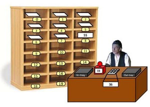
here .
Let us write a memory module (RAM) consisting of four (ADDR_WIDTH = 2) four-bit (DATA_WIDTH = 4) words. Data is loaded into RAM from data_in at adr when the clock signal clk arrives.
module R0 #(parameter ADDR_WIDTH = 2, DATA_WIDTH = 4) ( input clk, // input [ADDR_WIDTH-1:0] adr, // input [DATA_WIDTH-1:0] data_in, // output [DATA_WIDTH-1:0] RAM_out // ); reg [DATA_WIDTH-1:0] mem [2**ADDR_WIDTH-1:0]; // mem always @(posedge clk) // clk mem [adr] <= data_in; // data_in assign RAM_out = mem[adr]; // RAM_out endmodule
In testbenche, we will load 0001 at address 00, 0010 at address 01, 0100 at address 10, 1000 at address 11:
Creating a testbenchCreate a new project, create files R0.v and tR0.v (these files will automatically be added to the project).
Compile both files.
Run simulated compiled tR0.v file
module tR0; reg clk; reg [1:0] adr; reg [3:0] data_in; wire [3:0] RAM_out; R0 test_R0 (clk, adr, data_in,RAM_out); initial begin clk = 0; adr[0] = 0; adr[1] = 0; data_in[0] = 0; data_in[1] = 0; data_in[2] = 0; data_in[3] = 0; #5 data_in[0] = 1; #5 clk = 1; #5 adr[0] = 1; data_in[0] = 0; data_in[1] = 1; clk = 0; #5 clk = 1; #5 adr[0] = 0; adr[1] = 1; data_in[1] = 0; data_in[2] = 1; clk = 0; #5 clk = 1; #5 adr[0] = 1; adr[1] = 1; data_in[2] = 0; data_in[3] = 1; clk = 0; #5 clk = 1; #5 adr[0] = 0; adr[1] = 0; data_in[3] = 0; clk = 0; #5 adr[0] = 1; adr[1] = 0; #5 adr[0] = 0; adr[1] = 1; #5 adr[0] = 1; adr[1] = 1; #5 adr[0] = 0; adr[1] = 0; #5 adr[0] = 1; adr[1] = 0; #5 adr[0] = 0; adr[1] = 1; #5 adr[0] = 1; adr[1] = 1; #5 adr[0] = 0; adr[1] = 0; #5 adr[0] = 1; adr[1] = 0; #5 adr[0] = 0; adr[1] = 1; #5 adr[0] = 1; adr[1] = 1; end endmodule

Connect the counter to the address input of the RAM. At the input of the counter you need to connect a clock generator.
Here is an example of a program using the ALTUFM_OSC internal generator. The frequency of the standard generator 5.5 MHz (MAX II EPM240 CPLD Minimal Development Board).
module inner_Clock ( output reg LED); ALTUFM_OSC osc( .oscena(1'b1), .osc(clk)); reg signal; reg [24:0] osc_counter; reg [24:0] const_data = 25'b10110111000110110000000; initial begin signal = 1'b0; osc_counter = 25'b0; end // 6 000 000 osc_counter always @(posedge clk) begin osc_counter <= osc_counter+ 1'b1; if(osc_counter == const_data) begin signal <= ~signal; osc_counter <= 25'b0; end LED = signal; // LED ~1 . end endmodule
You can also use an external generator, for example, a CMOS 555 timer (running from 3.3V). We connect the timer 555 to the counter, we connect the counter to the address input of the RAM.
So when the clock signal arrives at the counter, we will move to the next cell in memory. Connect the RAM_button button to the clock input of the RAM - the data in the RAM will be loaded when you click on this button.
module R1 (timer555, RAM_button, data_in, RAM_out, counter); parameter ADDR_WIDTH = 2; parameter DATA_WIDTH = 4; input timer555; input RAM_button; //input [ADDR_WIDTH-1:0] adr; input [DATA_WIDTH-1:0] data_in; output [DATA_WIDTH-1:0] RAM_out; output reg [1:0] counter; // Counter always @(posedge timer555) counter <= counter + 1; // RAM wire [ADDR_WIDTH-1:0] adr; assign adr = counter; reg [DATA_WIDTH-1:0] mem [2**ADDR_WIDTH-1:0]; always @(posedge RAM_button) mem [adr] <= data_in; assign RAM_out = mem[adr]; endmodule
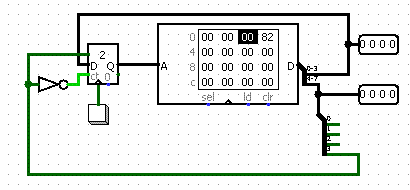
Here is the scheme in RTL Viewer

In the ModelSim simulator, this scheme will not work, because the counter is not initialized. The efficiency of the scheme can be checked by directly loading the program into the FPGA.
Next, add the download function to the counter. Loading from data_in [1: 0] is done by clicking on the Counter_load button
module R2 (counter, timer555, Counter_load, RAM_button, data_in, RAM_out); parameter ADDR_WIDTH = 2; parameter DATA_WIDTH = 4; output [1:0] counter; input timer555, Counter_load; // input [N-1:0] adr; input RAM_button; input [DATA_WIDTH-1:0] data_in; output [DATA_WIDTH-1:0] RAM_out; // Counter reg [1:0] counter; always @ (posedge timer555 or posedge Counter_load) if (Counter_load) counter <= data_in[1:0]; else counter <= counter + 2'b01; // RAM wire [ADDR_WIDTH-1:0] adr; assign adr = counter; reg [DATA_WIDTH-1:0] mem [2**ADDR_WIDTH-1:0]; always @(posedge RAM_button) mem [adr] <= data_in; assign RAM_out = mem[adr]; endmodule
Here is the connection of buttons and LEDs in Pin Planner:

Download 0001 at address 00, 0010 at address 01, 0100 at address 10, 1000 at address 11
module tR2; parameter ADDR_WIDTH = 2; parameter DATA_WIDTH = 4; reg timer555, Counter_load, RAM_button; wire [1:0] counter; reg [DATA_WIDTH-1:0] data_in; wire [DATA_WIDTH-1:0] RAM_out; R2 test_R2(counter, timer555, Counter_load, RAM_button, data_in, RAM_out); initial // Clock generator begin timer555 = 0; forever #20 timer555 = ~timer555; end initial begin data_in[0] = 0; data_in[1] = 0; data_in[2] = 0; data_in[3] = 0; Counter_load = 0; RAM_button = 0; #5 data_in[0]=0; data_in[1]=0; Counter_load=1; RAM_button=0; #5 data_in[0]=1; data_in[1]=0; Counter_load=0; RAM_button=1; #5 data_in[0]=0; data_in[1]=0; Counter_load=0; RAM_button=0; #5 data_in[0]=1; data_in[1]=0; Counter_load=1; RAM_button=0; #5 data_in[0]=0; data_in[1]=1; Counter_load=0; RAM_button=1; #5 data_in[0]=0; data_in[1]=0; Counter_load=0; RAM_button=0; #5 data_in[0]=0; data_in[1]=1; Counter_load=1; RAM_button=0; #5 data_in[2]=1; data_in[0]=0; data_in[1]=0; Counter_load=0; RAM_button=1; #5 data_in[2]=0; data_in[0]=0; data_in[1]=0; Counter_load=0; RAM_button=0; #5 data_in[0]=1; data_in[1]=1; Counter_load=1; RAM_button=0; #5 data_in[3]=1; data_in[0]=0; data_in[1]=0; Counter_load=0; RAM_button=1; #5 data_in[3]=0; data_in[0]=0; data_in[1]=0; Counter_load=0; RAM_button=0; end endmodule

In a separate module, create a 4bit register (battery).
Data is loaded into the register when you press the reg_button button:
module register4 ( input [3:0] reg_data, input reg_button, output reg [3:0] q ); always @(posedge reg_button) q <= reg_data; endmodule
Add to the general scheme Acc battery, MUX2 multiplexer and sum adder.
The adder adds to the number in the battery Acc numbers from the memory.
The data inputs of the multiplexer are served by the data_in and sum numbers.
The number of MUX2 is loaded into the Acc battery when you press the Acc_button button.
The number from Ass is loaded into RAM when the RAM_button button is pressed.

module R3 (MUX_switch, Acc_button, Acc, counter, timer555, Counter_load, RAM_button, data_in, RAM_out); parameter ADDR_WIDTH = 2; parameter DATA_WIDTH = 4; input MUX_switch; input Acc_button; output [3:0] Acc; input timer555, Counter_load; output [1:0] counter; // input [N-1:0] adr; input RAM_button; input [DATA_WIDTH-1:0] data_in; output [DATA_WIDTH-1:0] RAM_out; // Counter reg [1:0] counter; always @ (posedge timer555 or posedge Counter_load) if (Counter_load) counter <= data_in[1:0]; else counter <= counter + 2'b01; // RAM wire [ADDR_WIDTH-1:0] adr; assign adr = counter; reg [DATA_WIDTH-1:0] mem [2**ADDR_WIDTH-1:0]; always @(posedge RAM_button) mem [adr] <= Acc; assign RAM_out = mem[adr]; // sum wire [3:0] sum; assign sum = Acc + RAM_out; // MUX2 reg [3:0] MUX2; always @* MUX2 = MUX_switch ? sum : data_in; // Acc_button /* reg Acc_dff; always @(posedge Acc_button or negedge timer555) if (!timer555) Acc_dff <= 1'b0; else Acc_dff <= timer555; */ //Acc register4 Acc_reg( .reg_data(MUX2), //.reg_button(Acc_dff), .reg_button(Acc_button), .q(Acc) ); endmodule
For software suppression bounce you can use a simple scheme given in the comments.
Next, we will add numbers, for example, 2 and 3.
1. We load numbers into the RAM
2. Zero Ass
3. Switch MUX2
4. We load the first number from the RAM in the Ass
5. We add to the number in the Ass the second number from the RAM
6. Download the amount in RAM
module tR3; parameter ADDR_WIDTH = 2; parameter DATA_WIDTH = 4; reg MUX_switch; reg Acc_button; wire [3:0] Acc; reg timer555, Counter_load, RAM_button; wire [1:0] counter; reg [DATA_WIDTH-1:0] data_in; wire [DATA_WIDTH-1:0] RAM_out; R3 test_R3(MUX_switch, Acc_button, Acc, counter, timer555, Counter_load, RAM_button, data_in, RAM_out); initial begin timer555 = 0; forever #20 timer555 = ~timer555; end initial begin data_in[0] = 0; data_in[1] = 0; data_in[2] = 0; data_in[3] = 0; Counter_load = 0; Acc_button = 0; RAM_button = 0; MUX_switch = 0; #5 Counter_load = 1; #5 data_in[0]=0; data_in[1]=1; Counter_load = 0; #5 Acc_button = 1; #5 RAM_button = 1; #5 data_in[0]=0; data_in[1] = 0; Acc_button = 0; RAM_button = 0; #5 data_in[0]=1; data_in[1]=1; #15 Acc_button = 1; #5 RAM_button = 1; #5 Acc_button = 0; #5 data_in[0]=0; data_in[1] = 0; RAM_button = 0; #10 Acc_button = 1; #10 Acc_button = 0; #60 MUX_switch = 1; #10 Acc_button = 1; #10 Acc_button = 0; #30 Acc_button = 1; #10 Acc_button = 0; #30 RAM_button = 1; #10 RAM_button = 0; end endmodule

Add an element to the main module that subtracts the number stored in the memory from the number in the battery.
wire [3:0] subtract; assign subract = Acc - RAM_out ;
Replace the two-input multiplexer with a four-input
always @* MUX4 = MUX_switch[1] ? (MUX_switch[0] ? RAM_out : subtract) : (MUX_switch[0] ? sum : data_in);
Connect the output device to the battery (4bit register), also connect 2 flags to the battery:
1. The "Zero" flag is a log. element 4ILE or NOT. The flag is raised if the contents of the ass is zero.
2. The “Zero or Positive Number” flag is a log. the item is NOT on the high-order discharge of the four-digit battery. The flag is raised if the contents of the Ass is greater than or equal to zero.
// "" output Z_flag; assign Z_flag = ~(|Acc); // // " " output PZ_flag; assign PZ_flag = ~Acc[3];
Add three teams
1. load the contents of the battery to the data_out
2. loading the address into the counter if the zero flag is raised (JMP if Acc = 0)
3. loading the address into the counter, if the “zero or positive number” flag is raised (JMP if Acc> = 0)
module R4 (JMP,Z_JMP,PZ_JMP,Z_flag,PZ_flag,Output_button,data_out,MUX_switch,Acc_button,Acc,counter,timer555,RAM_button,data_in,RAM_out); parameter ADDR_WIDTH = 2; parameter DATA_WIDTH = 4; input JMP, Z_JMP, PZ_JMP; output Z_flag, PZ_flag; input Output_button; output [3:0] data_out; input [1:0] MUX_switch; input Acc_button; output [3:0] Acc; input timer555; output [1:0] counter; input RAM_button; input [DATA_WIDTH-1:0] data_in; output [DATA_WIDTH-1:0] RAM_out; // flags wire Z,PZ; assign Z = Z_flag & Z_JMP; assign PZ = PZ_flag & PZ_JMP; // Counter reg [1:0] counter; always @ (posedge timer555 or posedge JMP or posedge Z or posedge PZ) if (JMP|Z|PZ) counter <= data_in[1:0]; else counter <= counter + 2'b01; // RAM wire [ADDR_WIDTH-1:0] adr; assign adr = counter; reg [DATA_WIDTH-1:0] mem [2**ADDR_WIDTH-1:0]; always @(posedge RAM_button) mem [adr] <= Acc; assign RAM_out = mem[adr]; // sum wire [3:0] sum; assign sum = Acc + RAM_out; //subtract wire [3:0] subtract; assign subtract = Acc - RAM_out; // MUX4 reg [3:0] MUX4; always @* MUX4 = MUX_switch[1] ? (MUX_switch[0] ? RAM_out : subtract) : (MUX_switch[0] ? sum : data_in); //Acc register4 Acc_reg( .reg_data(MUX4), .reg_button(Acc_button), .q(Acc) ); //data_out register4 Output_reg( .reg_data(Acc), .reg_button(Output_button), .q(data_out) ); assign Z_flag = ~(|Acc); assign PZ_flag = ~Acc[3]; endmodule
1. We load numbers into the RAM
2. Zero Ass
3. Switch MUX2
4. Subtract the first number (recorded in RAM) from Ass
5. Subtract the second number (recorded in RAM) from Ass
6. We load the amount in RAM and data_out
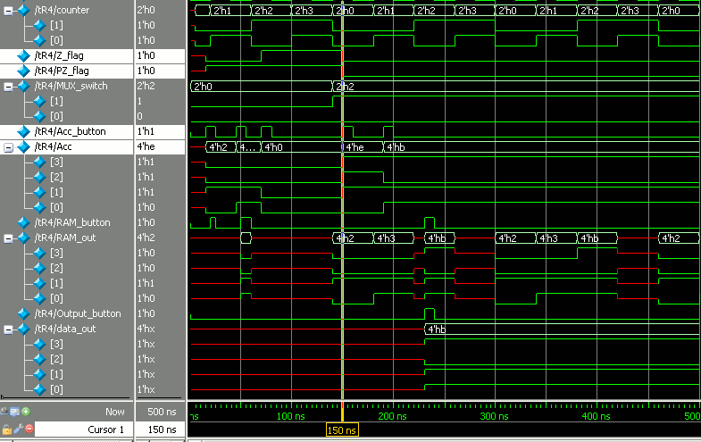
module tR4; parameter ADDR_WIDTH = 2; parameter DATA_WIDTH = 4; reg JMP, Z_JMP, PZ_JMP; wire Z_flag, PZ_flag; reg Output_button; wire [3:0] data_out; reg [1:0] MUX_switch; reg Acc_button; wire [3:0] Acc; reg timer555, RAM_button; wire [1:0] counter; reg [DATA_WIDTH-1:0] data_in; wire [DATA_WIDTH-1:0] RAM_out; R4 test_R4 (JMP,Z_JMP,PZ_JMP,Z_flag,PZ_flag,Output_button,data_out,MUX_switch,Acc_button,Acc, counter,timer555,RAM_button,data_in,RAM_out); initial begin timer555 = 0; forever #20 timer555 = ~timer555; end initial begin data_in[0] = 0; data_in[1] = 0; data_in[2] = 0; data_in[3] = 0; JMP = 0; Z_JMP = 0; PZ_JMP = 0; Acc_button = 0; RAM_button = 0; Output_button = 0; MUX_switch[0] = 0; MUX_switch[1] = 0; #5 JMP = 1; #5 data_in[0]=0; data_in[1]=1; JMP = 0; #5 Acc_button = 1; #5 RAM_button = 1; #5 data_in[0]=0; data_in[1] = 0; Acc_button = 0; RAM_button = 0; #5 data_in[0]=1; data_in[1]=1; #15 Acc_button = 1; #5 RAM_button = 1; #5 Acc_button = 0; #5 data_in[0]=0; data_in[1] = 0; RAM_button = 0; #10 Acc_button = 1; #10 Acc_button = 0; #60 MUX_switch[1] = 1; #10 Acc_button = 1; #10 Acc_button = 0; #30 Acc_button = 1; #10 Acc_button = 0; #30 RAM_button = 1; Output_button = 1; #10 RAM_button = 0; Output_button = 0; end endmodule
Let us verify that when a positive number lies in Ass, the Z_JMP transition does not occur:
module tR4_jmp; parameter ADDR_WIDTH = 2; parameter DATA_WIDTH = 4; reg JMP, Z_JMP, PZ_JMP; wire Z_flag, PZ_flag; reg Output_button; wire [3:0] data_out; reg [1:0] MUX_switch; reg Acc_button; wire [3:0] Acc; reg timer555, RAM_button; wire [1:0] counter; reg [DATA_WIDTH-1:0] data_in; wire [DATA_WIDTH-1:0] RAM_out; R4 test_R4 (JMP,Z_JMP,PZ_JMP,Z_flag,PZ_flag,Output_button,data_out,MUX_switch,Acc_button,Acc, counter,timer555,RAM_button,data_in,RAM_out); initial begin timer555 = 0; forever #20 timer555 = ~timer555; end initial begin data_in[0] = 0; data_in[1] = 0; data_in[2] = 0; data_in[3] = 0; JMP = 0; Z_JMP = 0; PZ_JMP = 0; Acc_button = 0; RAM_button = 0; Output_button = 0; MUX_switch[0] = 0; MUX_switch[1] = 0; #5 JMP = 1; #5 data_in[0]=0; data_in[1]=1; JMP = 0; #5 Acc_button = 1; #5 data_in[0]=1; data_in[1]=1; Acc_button = 1; #5 data_in[0]=1; data_in[1]=1; Acc_button = 0; #5 Z_JMP = 1; #5 PZ_JMP = 1; Z_JMP = 0; #5 PZ_JMP = 0; end endmodule

Let's place the unconditional jump command in the RAM
View design
//wire Counter_load; always @ (posedge timer555) if (Counter_load) counter <= RAM_out[3:0]; else counter <= counter + 2'b01;
will not work in ModelSim, so we will use the additional reset_count command, which initializes the counter, resetting it, i.e.
module resCount (reset_count, counter, timer555, RAM_button, data_in, RAM_out); parameter ADDR_WIDTH = 4; parameter DATA_WIDTH = 8; input reset_count; output [ADDR_WIDTH-1:0] counter; input timer555; input RAM_button; input [DATA_WIDTH-1:0] data_in; output [DATA_WIDTH-1:0] RAM_out; wire Counter_load; assign Counter_load = RAM_out[7]; reg [ADDR_WIDTH-1:0] counter; always @ (posedge timer555 or posedge reset_count) if (reset_count) counter <= 4'b0000; else if (Counter_load) counter <= RAM_out[3:0]; else counter <= counter + 4'b0001; wire [ADDR_WIDTH-1:0] adr; assign adr = counter; reg [DATA_WIDTH-1:0] mem [2**ADDR_WIDTH-1:0]; always @(posedge RAM_button) mem [adr] <= data_in; assign RAM_out = mem[adr]; endmodule
test bench
module tresCount; parameter ADDR_WIDTH = 4; parameter DATA_WIDTH = 8; reg reset_count; reg timer555, RAM_button; wire [ADDR_WIDTH-1:0] counter; reg [DATA_WIDTH-1:0] data_in; wire [DATA_WIDTH-1:0] RAM_out; resCount test_resCount(reset_count, counter, timer555, RAM_button, data_in, RAM_out); initial // Clock generator begin timer555 = 0; forever #20 timer555 = ~timer555; end initial begin data_in[0] = 0; data_in[1] = 0; data_in[2] = 0; data_in[3] = 0; data_in[4] = 0; data_in[5] = 0; data_in[6] = 0; data_in[7] = 0; RAM_button = 0; reset_count =1; #5 reset_count =0; #1500 data_in[7] =1; #5 RAM_button = 1; #5 data_in[7] =0; RAM_button = 0; end endmodule
Add to the scheme MUX2 and Ass. We will write to Ass with the RAM_out command [6].
assign Acc_button = RAM_out[6];
To the clock input Ass connect log. element and
// regiser4 (posedge reg_button) (negedge reg_button) .reg_button(Acc_button & timer555),
The meaning of the connection log. element And to the clock input in that now on the front of timer555 you can switch the multiplexer, and on the decline to write to the battery. So we put two teams in one beat.
We will switch MUX2 with the command RAM_out [5]
assign MUX_switch = RAM_out[5];

module register4 ( input [3:0] reg_data, input reg_button, output reg [3:0] q ); always @(negedge reg_button) // "posedge" "negedge" q <= reg_data; endmodule module R50 (reset_count, counter, timer555, RAM_button, data_in, RAM_out, mux_switch_out, mux_out,Acc_out); parameter ADDR_WIDTH = 2; parameter DATA_WIDTH = 8; input reset_count; output [ADDR_WIDTH-1:0] counter; input timer555; input RAM_button; input [DATA_WIDTH-1:0] data_in; output [DATA_WIDTH-1:0] RAM_out; output [3:0] Acc_out; output mux_switch_out; output [3:0] mux_out; wire Counter_load; assign Counter_load = RAM_out[7]; //Counter reg [ADDR_WIDTH-1:0] counter; always @ (posedge timer555 or posedge reset_count) if (reset_count) counter <= 2'b00; else if (Counter_load) counter <= RAM_out[1:0]; else counter <= counter + 2'b01; wire [ADDR_WIDTH-1:0] adr; assign adr = counter; //RAM reg [DATA_WIDTH-1:0] mem [2**ADDR_WIDTH-1:0]; always @(posedge RAM_button) mem [adr] <= data_in; assign RAM_out = mem[adr]; // MUX2 wire MUX_switch; assign MUX_switch = RAM_out[5]; reg [3:0] MUX2; always @* MUX2 = MUX_switch ? RAM_out : data_in[3:0]; // 4 data_in assign mux_out = MUX2; assign mux_switch_out = MUX_switch; wire Acc_button; assign Acc_button = RAM_out[6]; //Acc register4 Acc_reg( .reg_data(mux_out), .reg_button(Acc_button & timer555), .q(Acc_out) ); endmodule
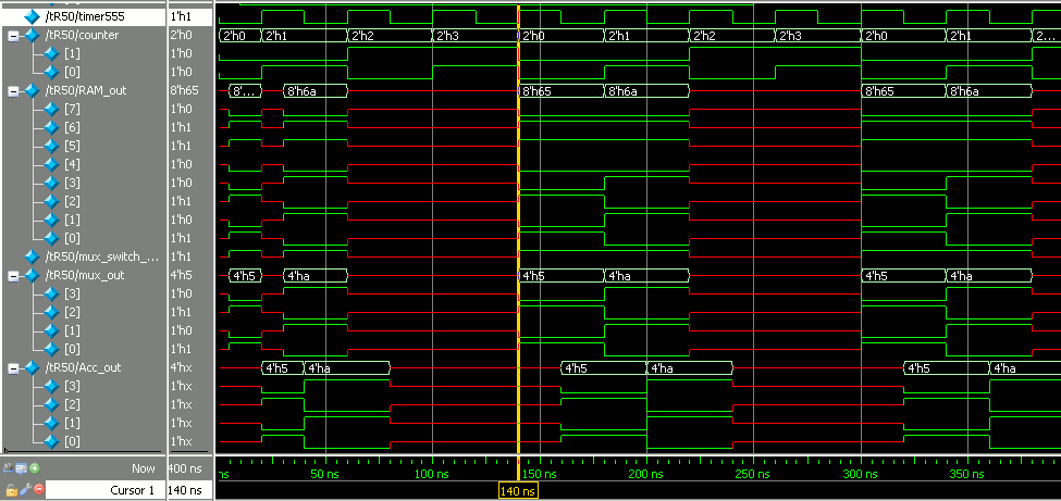
In the testbench, write the number 0101 in cell 00, and the number 1010 in cell 01; load these numbers into the battery
module tR50; parameter ADDR_WIDTH = 2; parameter DATA_WIDTH = 8; reg reset_count; reg timer555, RAM_button; wire [ADDR_WIDTH-1:0] counter; reg [DATA_WIDTH-1:0] data_in; wire [DATA_WIDTH-1:0] RAM_out; wire mux_switch_out; wire [3:0] mux_out; wire [3:0] Acc_out; R50 test_R50(reset_count, counter, timer555, RAM_button, data_in, RAM_out, mux_switch_out, mux_out,Acc_out); initial // Clock generator begin timer555 = 0; forever #20 timer555 = ~timer555; end initial begin data_in[0] = 1; data_in[1] = 0; data_in[2] = 1; data_in[3] = 0; data_in[4] = 0; data_in[5] = 1; data_in[6] = 1; data_in[7] = 0; RAM_button = 0; reset_count =1; #5 RAM_button = 1; reset_count = 0; #5 data_in[0]=0; data_in[2]=0; data_in[5]=0; data_in[6]=0; RAM_button=0; #15 data_in[1]=1; data_in[3]=1; data_in[5]=1;data_in[6]=1; #5 RAM_button=1; #5 data_in[1]=0; data_in[3]=0; data_in[5]=0; data_in[6]=0; RAM_button=0; end endmodule
Put the second RAM in the general scheme and we will write to RAM with the command RAM1_out [4].
assign RAM2_button = RAM1_out[4];

module register4 ( input [3:0] reg_data, input reg_button, output reg [3:0] q ); always @(negedge reg_button) q <= reg_data; endmodule module R51 (reset_count, counter, timer555, RAM1_button, data_in, RAM1_out, RAM2_out, mux_switch_out, mux_out,Acc_out); parameter ADDR_WIDTH = 3; parameter DATA_WIDTH = 8; input reset_count; output [ADDR_WIDTH-1:0] counter; input timer555; input RAM1_button; input [DATA_WIDTH-1:0] data_in; output [DATA_WIDTH-1:0] RAM1_out; output [3:0] RAM2_out; output [3:0] Acc_out; output mux_switch_out; output [3:0] mux_out; wire Counter_load; assign Counter_load = RAM1_out[7]; //Counter reg [ADDR_WIDTH-1:0] counter; always @ (posedge timer555 or posedge reset_count) if (reset_count) counter <= 2'b00; else if (Counter_load) counter <= RAM1_out[1:0]; else counter <= counter + 2'b01; wire [ADDR_WIDTH-1:0] adr1; assign adr1 = counter; //RAM1 reg [DATA_WIDTH-1:0] mem1 [2**ADDR_WIDTH-1:0]; always @(posedge RAM1_button ) mem1 [adr1] <= data_in; assign RAM1_out = mem1[adr1]; wire [ADDR_WIDTH-1:0] adr2; assign adr2 = RAM1_out[3:0]; wire RAM2_button; assign RAM2_button = RAM1_out[4]; //RAM2 reg [3:0] mem2 [2**ADDR_WIDTH-1:0]; always @(posedge RAM2_button) mem2 [adr2] <= Acc_out; assign RAM2_out = mem2[adr2]; // MUX2 wire MUX_switch; assign MUX_switch = RAM1_out[5]; reg [3:0] MUX2; always @* MUX2 = MUX_switch ? RAM2_out : data_in[3:0]; assign mux_out = MUX2; assign mux_switch_out = MUX_switch; wire Acc_button; assign Acc_button = RAM1_out[6]; //Acc register4 Acc_reg( .reg_data(mux_out), .reg_button(Acc_button & timer555), .q(Acc_out) ); endmodule
In the testbench we will load the numbers 0100 and 1000 from Ass to zero 0000 and the first 0001 cells of mem2 RAM (then we will load these numbers into Ass from RAM mem2)
module tR51; parameter ADDR_WIDTH = 3; parameter DATA_WIDTH = 8; reg reset_count; reg timer555, RAM1_button; wire [ADDR_WIDTH-1:0] counter; reg [DATA_WIDTH-1:0] data_in; wire [DATA_WIDTH-1:0] RAM1_out; wire [3:0] RAM2_out; wire mux_switch_out; wire [3:0] mux_out; wire [3:0] Acc_out; R51 test_R51(reset_count, counter, timer555, RAM1_button, data_in, RAM1_out, RAM2_out, mux_switch_out, mux_out,Acc_out); initial // Clock generator begin timer555 = 0; forever #20 timer555 = ~timer555; end initial begin data_in[0] = 0; data_in[1] = 0; data_in[2] = 0; data_in[3] = 0; data_in[4] = 0; data_in[5] = 0; data_in[6] = 1; data_in[7] = 0; RAM1_button = 0; reset_count =1; #5 RAM1_button = 1; reset_count = 0; #5 RAM1_button = 0; data_in[6] = 0; #10 data_in[4] = 1; #5 RAM1_button = 1; #5 data_in[4] = 0; RAM1_button = 0; #30 data_in[6] = 1; #5 RAM1_button = 1; #5 data_in[6] = 0; RAM1_button = 0; #30 data_in[4] = 1; data_in[0] = 1; #5 RAM1_button = 1; #5 data_in[4] = 0; data_in[0] = 0; RAM1_button = 0; #30 data_in[6] = 1; #5 RAM1_button = 1; #5 RAM1_button = 0; data_in[6] = 0; #30 data_in[5] = 1; data_in[6] = 1; #5 RAM1_button = 1; #5 RAM1_button = 0; data_in[5] = 0; data_in[6] = 0; #30 data_in[5] = 1; data_in[6] = 1; data_in[0] = 1; #5 RAM1_button = 1; #5 RAM1_button = 0; data_in[0] = 0; data_in[5] = 0; data_in[6] = 0; #70 data_in[2] = 1; #80 data_in[2] = 0; data_in[3] = 1; #40 data_in[3] = 0; end endmodule

I add that the scheme c log. element And on the clock input of the battery will not always work correctly (depends on the board). Replace the log. element And on the trigger Acc_dff, we will load the trigger on the negative front (on decay) of the timer555 clock signal, we will load the battery on the positive front
// Acc_dff reg Acc_dff; always @(negedge timer555) Acc_dff <= Acc_button;
So, adding the remaining commands, create a module R52 (LMC)

module register4 ( input [3:0] reg_data, input reg_button, output reg [3:0] q ); always @(posedge reg_button) // negedge -> posedge q <= reg_data; endmodule module R52 (Z_flag, PZ_flag, reset_count, counter, timer555, RAM1_button, data_in, RAM1_out, RAM2_out, mux_switch_out, mux_out, Acc_out, data_out, Acc_dff); parameter ADDR_WIDTH = 4; parameter DATA_WIDTH = 12; input reset_count; input timer555; input RAM1_button; input [DATA_WIDTH-1:0] data_in; output [ADDR_WIDTH-1:0] counter; output [1:0] mux_switch_out; output [3:0] mux_out; output [3:0] Acc_out; output [3:0] data_out; output [DATA_WIDTH-1:0] RAM1_out; output [3:0] RAM2_out; output Z_flag, PZ_flag; output Acc_dff; wire JMP_button, Z_JMP_button,PZ_JMP_button; assign JMP_button = RAM1_out[6]; assign Z_JMP_button = RAM1_out[5]; assign PZ_JMP_button = RAM1_out[4]; wire Z_JMP,PZ_JMP; assign Z_JMP = Z_flag & Z_JMP_button; assign PZ_JMP = PZ_flag & PZ_JMP_button; //Counter reg [ADDR_WIDTH-1:0] counter; always @ (posedge timer555 or posedge reset_count) if (reset_count) counter <= 4'b0000; else if (JMP_button|Z_JMP|PZ_JMP) counter <= RAM1_out[3:0]; else counter <= counter + 4'b0001; wire [ADDR_WIDTH-1:0] adr1; assign adr1 = counter; //RAM1 reg [DATA_WIDTH-1:0] mem1 [2**ADDR_WIDTH-1:0]; always @(posedge RAM1_button ) mem1 [adr1] <= data_in; assign RAM1_out = mem1[adr1]; //RAM2_adr wire [ADDR_WIDTH-1:0] adr2; assign adr2 = RAM1_out[2:0]; //RAM2_button wire RAM2_button; assign RAM2_button = RAM1_out[11]; //RAM2 reg [3:0] mem2 [2**ADDR_WIDTH-1:0]; always @(posedge RAM2_button) mem2 [adr2] <= Acc_out; assign RAM2_out = mem2[adr2]; // sum wire [3:0] sum; assign sum = Acc_out + RAM2_out; //subtract wire [3:0] subtract; assign subtract = Acc_out - RAM2_out; // MUX4 wire [1:0] mux_switch; assign mux_switch[0] = RAM1_out[7]; assign mux_switch[1] = RAM1_out[8]; reg [3:0] MUX4; always @* MUX4 = mux_switch[1] ? (mux_switch[0] ? RAM2_out : subtract) : (mux_switch[0] ? sum : data_in[3:0]); assign mux_out = MUX4; assign mux_switch_out[0] = mux_switch[0]; assign mux_switch_out[1] = mux_switch[1]; //Acc_button wire Acc_button; assign Acc_button = RAM1_out[10]; // Acc_dff reg Acc_dff; always @(negedge timer555) Acc_dff <= Acc_button; //Acc register4 Acc_reg( .reg_data(mux_out), //.reg_button(Acc_button & timer555), .reg_button(Acc_dff), .q(Acc_out) ); //data_out wire Output_button; assign Output_button = RAM1_out[9]; register4 Output_reg( .reg_data(Acc_out), .reg_button(Output_button), .q(data_out) ); // flags assign Z_flag = ~(|Acc_out); assign PZ_flag = ~Acc_out[3]; endmodule
In the testbench, we’ll check how the maximum number search algorithm works.
The peculiarity of loading commands into RAM is that after loading all the commands, we have to return (340ns) to cell 8 and load another command
module tR52; parameter ADDR_WIDTH = 4; parameter DATA_WIDTH = 12; reg reset_count; reg timer555; reg RAM1_button; reg [DATA_WIDTH-1:0] data_in; wire [ADDR_WIDTH-1:0] counter; wire [1:0]mux_switch_out; wire [3:0] mux_out; wire [3:0] Acc_out; wire [3:0] data_out; wire [DATA_WIDTH-1:0] RAM1_out; wire [3:0] RAM2_out; wire Z_flag, PZ_flag; wire Acc_dff; R52 test_R52(Z_flag, PZ_flag, reset_count, counter, timer555, RAM1_button, data_in, RAM1_out, RAM2_out, mux_switch_out, mux_out,Acc_out, data_out, Acc_dff); initial // Clock generator begin timer555 = 0; forever #20 timer555 = ~timer555; end initial begin data_in[0] = 0; data_in[1] = 0; data_in[2] = 0; data_in[3] = 0; data_in[4] = 0; data_in[5] = 0; data_in[6] = 0; data_in[7] = 0; data_in[8] = 0; data_in[9] = 0; data_in[10] = 1; data_in[11] = 0; RAM1_button = 0; reset_count =1; // 1- #5 RAM1_button = 1; reset_count = 0; #5 RAM1_button = 0; data_in[10] = 0; data_in[0] = 0; // 1- 0 #10 data_in[11] = 1; #5 RAM1_button = 1; #5 data_in[11] = 0; RAM1_button = 0; // 2- #30 data_in[10] = 1; #5 RAM1_button = 1; #5 RAM1_button = 0; data_in[10] = 0; // 2- 0 #30 data_in[11] = 1;data_in[0] = 1; #5 RAM1_button = 1; #5 data_in[11] = 0;data_in[0] = 0; RAM1_button = 0; // 1- #30 data_in[8]=1; data_in[10] = 1; #5 RAM1_button = 1; #5 RAM1_button = 0; data_in[8]=0; data_in[10] = 0; // Acc>=0, 8 #30 data_in[4]=1; data_in[3]=1; #5 RAM1_button = 1; #5 RAM1_button = 0; data_in[4]=0; data_in[3]=0; // 1- #30 data_in[7] = 1; data_in[8] = 1; data_in[10] = 1; #5 RAM1_button = 1; #5 RAM1_button = 0; data_in[7] = 0; data_in[8] = 0; data_in[10] = 0; // 9 #30 data_in[6] = 1; data_in[3]=1; data_in[0]=1; #5 RAM1_button = 1; #5 RAM1_button = 0; data_in[6] = 0; data_in[3]=0; data_in[0]=0; // data_out #30 data_in[9] = 1; #5 RAM1_button = 1; #5 RAM1_button = 0; data_in[9] = 0; // 8 #30 data_in[6] = 1; data_in[3]=1; data_in[0]=0; #5 RAM1_button = 1; #5 RAM1_button = 0; data_in[6] = 0; data_in[3]=0; data_in[0]=0; // 2- #30 data_in[7] = 1; data_in[8] = 1; data_in[10] = 1; data_in[0] = 1; #5 RAM1_button = 1; #5 RAM1_button = 0; data_in[7] = 0; data_in[8] = 0; data_in[10] = 0; data_in[0] = 0; #75 RAM1_button = 1; #5 RAM1_button = 0; #230 data_in[2]=1; data_in[0]=0; // #80 data_in[2]=0; data_in[0]=1; // end endmodule
Link to github with program codes.
The free student version of
ModelSim for Windows can be downloaded from
www.model.com .
Next, you need (by filling out the form) to download the student_license.dat file and place this file in the main directory of the
ModelSim program.
Link to the
ModelSim file for Linux (Ubuntu)
hereInstallation instructions
here .