A few days ago, Intel
announced that production problems (insufficient yield) forced it to shift the start of commercial production at design standards of 10 nm from the end of this year to the beginning of the next. And TSMC has already begun mass production of 7 nm, with five dozen projects this year. This is one side of the coin.
The other side is
yesterday's translation of an article about a schoolchild from the USA, who did what
BarsMonster failed , and produced a microchip in the garage. With design standards of 175 microns!
In the comments to this translation there were a number of questions “when is it already possible to buy an open-end processor?”, “When will 3D printers for microchips appear?”, And I decided to light up a bit the question of what happens to design standards between 10 nm and 175 µm , including in relation to their availability for fans and small companies.
Spoiler: ASIC for mining is very expensive (tens of millions of dollars).
Is something produced at all according to outdated design standards?What is the general design standards? In the classical sense, the phrase “design norms of X nanometers” meant that the gate length of the transistor is these same X nanometers. Starting from a certain moment (below 20 nm), the reduction in the size of transistors (also known as Moore's law) stopped working, it was necessary to invent various tricks (for example, FinFET), but marketers were relentless: the cherished number had to be moved further down. Therefore, in modern 10 nm processes, the actual channel length is still the same 20 nm. But more importantly, the first decades of its existence, Moore's law moved the semiconductor industry forward, not only because it was less steeper, but also because each transistor was cheaper in the next generation of design standards than in the previous generation. That is, for the same money on the crystal of the same size it was possible to put more functionality. But this ended, and 28 nm were design standards with the cheapest transistor, after which the transistors began to rise in price. This, in turn, led to the fact that for many applications to move to advanced design standards has become economically unprofitable. And this applies to industries where small project standards have traditionally been widely used, and there are also applications where they were not needed anyway.
Let's look at the sales cut of the world's largest factory TSMC (about half of the total market). From above one of quarters of 2015, from below - 2009.
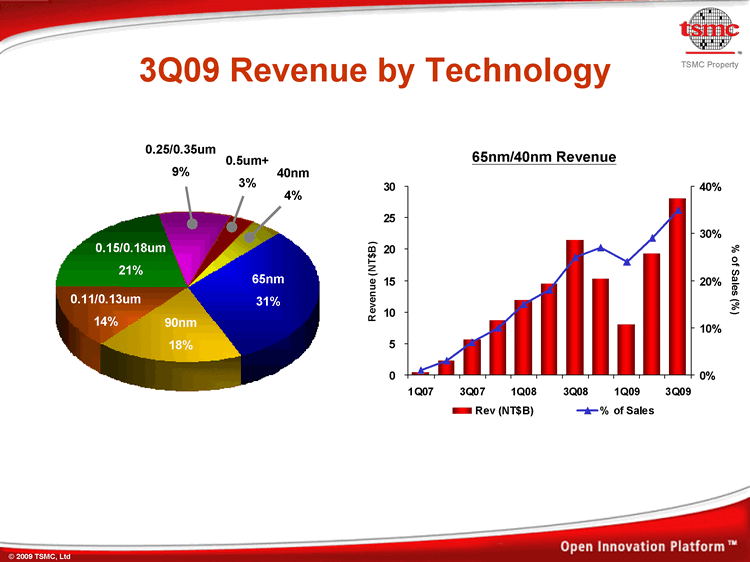
What do we see on these graphs? The fact that both in 2009 and in 2015 the two thinnest project standards brought TSMC only half of the total revenue, and that 15-20 percent bring technology from at least a decade ago! In the 2009 graph, there are 4% of 40 nm, but we will ignore them for simplicity, because these were the first weeks after the launch of the technology.
Another of these graphs shows that over seven years, the proportion of the 130/110 nm process technology has decreased eight times, 90 nm - five times, and 65 nm and 180/150 nm - only twice. This is especially clearly seen in the 2015 chart - with the growth of project norms, the sectors narrow, narrow, and then there is one broad sector.
I note that we are now talking about ten percent of the world's largest factory revenue, which is more than all the fourth-largest revenue and eight times as much of a respected player in the market as the German XFAB (which, by the way, no technology below 130 nm). How many times it is more than Zelenograd “Micron”, which also has design standards of 180 nm, I am even afraid to think.
At the same time, the market is growing, and the production according to the old design standards also applies. Moreover, new factories operating with “outdated” 200 mm plates are even being commissioned.
Why is that? To answer this question, let's go to the TSMC website,
in the “technology” section .
There we will see three subsections: “plans”, “logical technologies” and “special technologies”. Everything is clear with the plans, in the section of logic we will see a series sorted by design standards, but in the section “special technologies” ... design standards are not mentioned at all! The subsections are sorted by application, and it is in this part that the orders for microcircuits are collected for a variety of design standards. For example, the description of the technology section for analog circuits:
“The company's comprehensive analogue process portfolio for all applications including smartphones, tablets, automotive electronics, computers, audio, electronic equipment and home appliances.”
Think about it! In 2018, the world's largest factory, a legislator and a pioneer, routinely advertises production at 500 nm. Why? Because it is cost effective.
The cost of manufacturing an integrated circuit doubles with each new step of design standards, and the difference between 28 nm and 180 nm is dozens of times. When you design a video card, which you plan to sell hundreds of millions of pieces, the cost of the crystal is not so important (but, by the way, the cost of more expensive software, specific cases, etc.) plays a role, but if you are going to release only ten thousand of some tricky ASIC to control the DC / DC converter, the difference between 180 and 350 nm may well determine the payback of your product.
Especially if your product is not purely digital. The TSMC site is not very open to outsiders, but not one. We go to the
site of the factory XFAB , by the way, quite popular in Russia. There is a long list in the “technology” section, with several options for each design standards. One process is for analog circuits, another is for power circuits, the third one has built-in photodetectors ...
If you open the
datasheet of the XP018 process technology (180 nm), then we will see within a dozen types of transistors, and the same number of resistors and capacitors. In this case, pay attention to the limiting value of Vgs - the voltage at the gate of the transistor, there will be not only and not so much expected for 180 nm 1.8 volts, but 5 volts! In fact, this technical process is not only 180 nm, 180 nm transistors for fast and low-power logic, 500 nm transistors for analog and input / output circuits, and 1000 nm power switches capable of work with voltages in tens of volts. And TSMC on the same crystal can have 90, 65 and 40 nm transistors, which differ not only in geometry, but also in doping levels and gate dielectric thickness, which determine the operating modes of the transistor. The total cost of chip production is usually comparable to the thinnest design standards available on it: the cost of masks for photolithography non-linearly increases with decreasing design standards, but additional masks for coarser options increase the cost linearly, by a few percent each.
But what if the main part of your project is occupied by high-voltage transistors, and quite a bit of logic? If you can tolerate the transfer of logic from 40 nm to 180, or from 180 to 600, you can save a lot. And after the removal of 180 nm of logic, the XP018 technical process magically turns into the
XHB06 technical process with design standards of 600 nm, and at the same time it becomes significantly cheaper to produce.
It is from here that a good load of such hopelessly outdated technologies is taken: the world requires not only new processors for mobile phones, but also new drivers for LEDs in a flash, control circuits for unmanned vehicle electromotive devices, and just microcontrollers for dummies and washing machines. And, for example, for such a rapidly growing market as the Internet of things, it is not so much the productivity that is important as the low power consumption that advanced technologies cannot boast of. And the same TSMC is now actively developing not only the 5 nm process technology, but also new options for the 20 nm process, which will make new generations of devices for IoT better and cheaper.
Here, for example, Global Foundries advertising about their technology for the IoT chips, there are a dozen technical processes, from 22 to 180 nm. About 7-10 speech does not go).
 How much and where to get?
The first and most important thing to understand is that a lot of money (tens or hundreds of thousands of dollars a year) costs CAD. But there is good news. If you do not consider the options of piracy, then, firstly, a number of universities have licenses for CAD (who knows, maybe it’s time to visit alma mater), and secondly, you can assemble a design route from large degrees of design convenience at large design standards and university bodies. There is
Electric VLSI (completely free, GNU), there is a
Magic topology editor, there is a
verilog Icarus simulator and in fact quite a lot more. The most difficult thing is to check the compliance of the topology with the design rules (DRC) and check the compliance of the topology and the scheme (LVS), but at 180-350-600 nm it is quite normal to make them in the same Electric VLSI.
It is also useful to go to
Opencores.org and see there are quite a few ready-made and semi-ready projects of varying degrees of complexity. Here, for example, you can find the open-source and already tested in silicon processor architecture
OpenRISC .
How much is the production?The most difficult question here is not even where to get the money, but how to make the factory talk to you at all. There is a special conversation about Russian realities, it is useless to go to the Micron, but more than a dozen of people, pretending from the times of Brezhnev, have survived, perhaps more than a dozen of them, can burn out. As for foreign factories, with a 100% probability you will need a legal entity, and even with it, most factories will think, ask about your plans for mass production, etc. etc. Most, but not all, so you can try. And yet you can still go to the alma mater and try to do through them, to the universities and the attitude is always good, and prices may well be more loyal.
In any case, to test the design performance before launching into a series, most factories have the MPW (Multi-Project Wafer) service - for quite modest money, they give you an area (usually from 9-10 to 25 square millimeters), then they collect many, many projects together, produce and give each participant a few dozen chips. This is a standard production route used by small companies around the world. The cost of MPW for design standards of 180-600 nm for different factories is in the range of 500-1500 euros per square millimeter, production takes 3-6 months. A small production batch will probably cost between 50 and 200 thousand euros, depending on the factory, the specifics of the project, etc. etc.
For design standards 28–20 and beyond, we will be talking about hundreds of thousands of euros for a test launch and millions for mass production.
Examples of prices for MPW can be found on the website of the major university aggregator
Europractice . Of course, it is necessary to take into account that these are prices for universities, but the difference with prices for mere mortals is not very big.
For a startup, it is quite realistic to find ten thousand euros for a launch (but, of course, in this case it is only one and not the biggest item of expenditure), but for an amateur it’s probably a little expensive. But ten square millimeters is actually a lot, and you can probably try to join a university project or find several other enthusiasts and get a startup to get some projects implemented on a single chip. Again, it is in any case cheaper than collecting your own production in the garage, and technical fun you will end up with packaging (if not ordered at the factory), development boards, and measuring equipment.
And finally - just a little about the "3D-printers for chips." A classic set of equipment for production costs from several hundred million dollars to several tens of billions, and the same amount will have to be invested in suitable premises, but for quite a long time in Japan a
Minimal Fab project is being developed, the ultimate goal of which is the possibility of producing microcircuits at least individually, without a clean room complex infrastructure requirements, and fewer orders of magnitude less money. If everything works out, it will become a very important milestone in the history of the semiconductor industry, and make it much more accessible and flexible.

So, according to the authors, it will look.
I do not follow this project in detail, but last year his representatives were already at Russian industry exhibitions and conferences, and negotiated deliveries. As far as I understand, now they are already close to ensuring a full production cycle, and we are talking about design standards in the range between 500 and 100 nm.