Foreword
I am very happy to tell you in detail about my first integrated circuit and share the vicissitudes of this project, which I was engaged in over the past year. I hope my success will inspire others and help start a revolution in the production of home chips. When I started this project, I had no idea what I got involved in, but in the end I found out more than I ever thought about physics, chemistry, optics, electronics, and many other fields.
In addition, my efforts were accompanied by only the most positive feedback and support from around the world. I am sincerely grateful to everyone who helped me, gave advice and inspired this project. Especially my amazing parents, who not only always support and encourage me as much as they can, but also provided me with a workplace and put up with electricity costs ... Thank you!
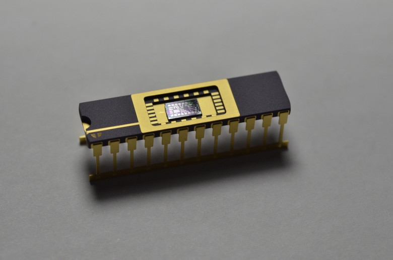
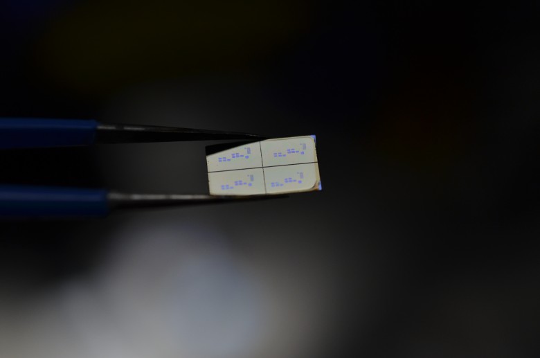
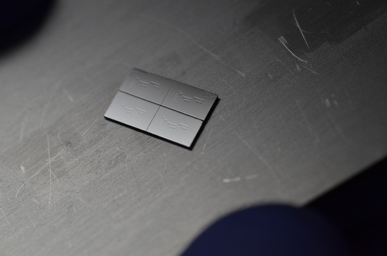
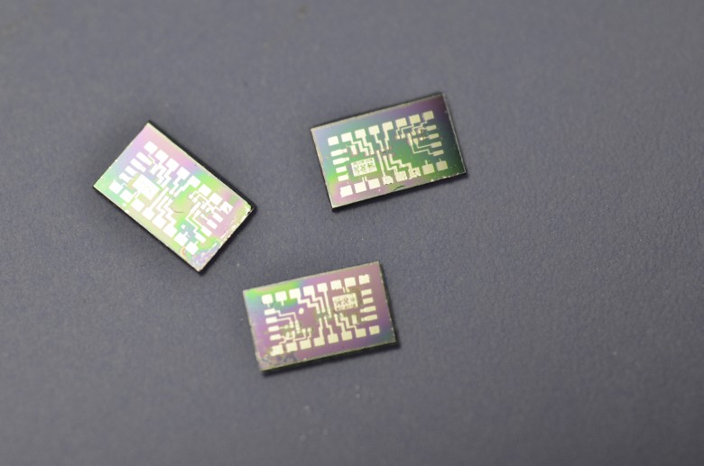
Without further ado, I present the first integrated circuit (IC) made by the lithographic method in home (garage) conditions — the PMOS chip of the Z1 dual differential amplifier.
I say "lithographically made" because Jerry Ellsworth manufactured the first transistors and logic gates (with connections carefully laid by hand with conductive epoxy) and showed the world that this is possible. Inspired by her work, I present integrated circuits created by a scalable, standard photolithographic process. Needless to say, this is a logical step forward compared to my previous work, where I
reproduced the Jerry field effect transistor .
Design
I
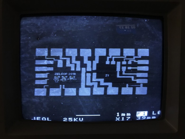
designed the Z1 amplifier when I was looking for a simple chip for testing and tuning my process. Layout made in
Magic VLSI for PMOS process with four masks (active / alloyed area, gate oxide, contact window and top metal layer). PMOS has an advantage over NMOS, given the ionic impurities due to manufacturing in the garage. The masks are designed with an aspect ratio of 16: 9 to simplify the projection.
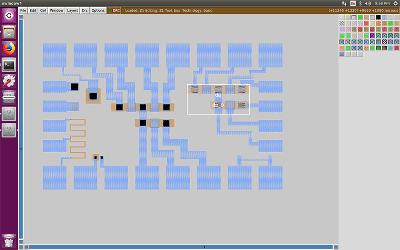 Layout Magic VLSI
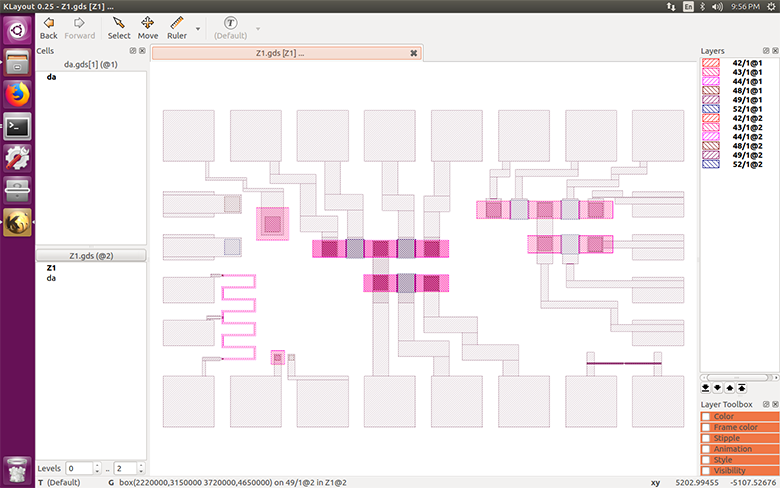 Mask generation
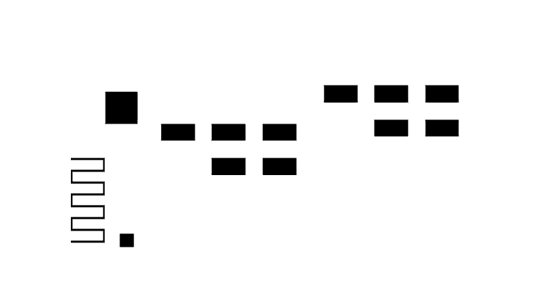 Active area
 Gate
Gate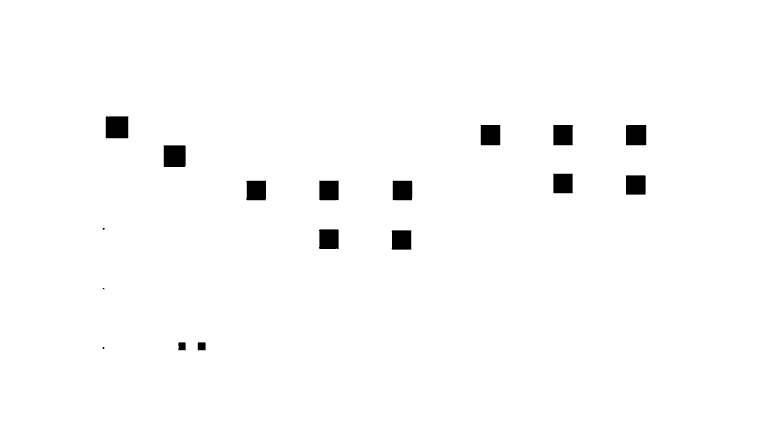 Contact
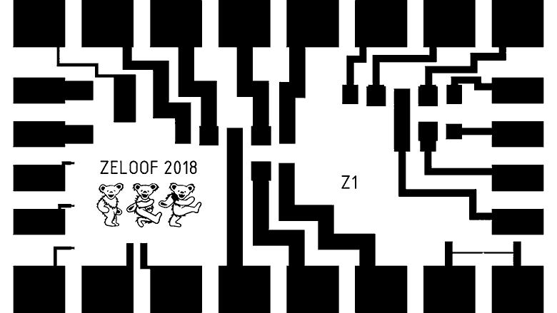 Metal
MetalThe shutter size is approximately 175 microns, although elements up to 2 microns in size are made on the chip for testing. Each amplifier section (center and right) contains three transistors (two for a
push-pull circuit with a common cathode resistance and one as a current source / load resistor), which means a total of six transistors on the IC. On the left side there are resistors, capacitors, diodes and other test elements to study the characteristics of the process. Each node of differential pairs comes out with a separate pin on the lead frame; therefore, it can be studied and, if necessary, an external offset can be added.
Manufacturing
The manufacturing process consists of 66 individual steps and takes approximately 12 hours. The yield reaches 80% for large items, but depends heavily on the amount of coffee consumed on a particular day. I also recorded a video on YouTube about the
theory of chip production and
separately about the manufacture of MOS transistors .
Silicon wafers 50 mm (2 ") are broken into 5.08 × 3.175 mm crystals (about 16 mm² in area)
with an Epilog fiber laser . Such a crystal size is chosen to fit into a 24-pin Kyocera DIP package.
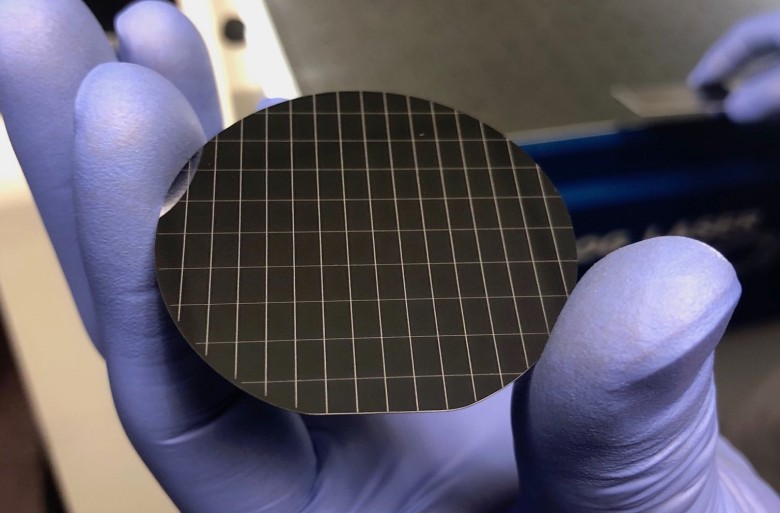 N-type plate 50 mm
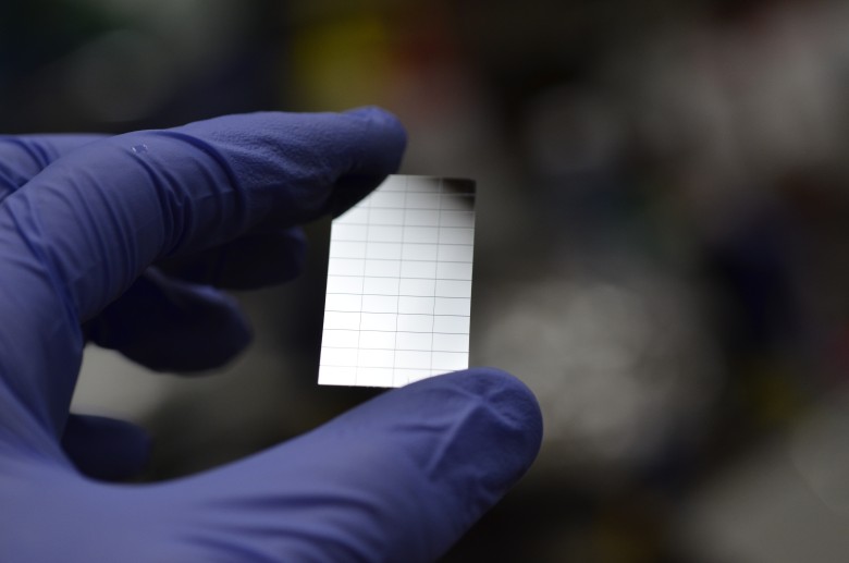 N-type plate 50 mm
First, the native oxide is removed from the plate by rapid immersion in dilute hydrogen fluoride followed by intensive treatment with an etching mixture “piranha” (a mixture of sulfuric acid and hydrogen peroxide), a mixture of RCA 1 (water, ammonia, hydrogen peroxide), a mixture of RCA 2 (water, hydrochloric acid, hydrogen peroxide) and re-immersion in hydrogen fluoride.
The protective oxide is
thermally grown in water vapor of ambient air (wet oxidation) to a thickness of 5000–8000 Å.
 Wet thermal oxidation
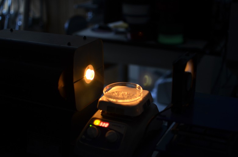 Wet thermal oxidation
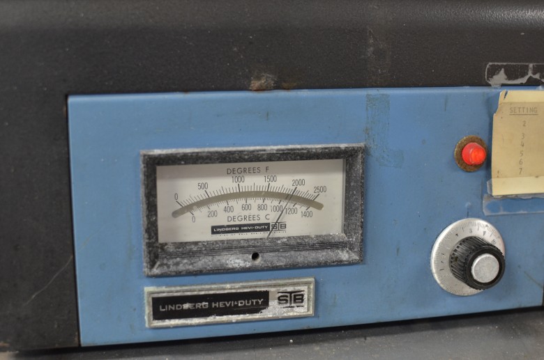 Tube furnace
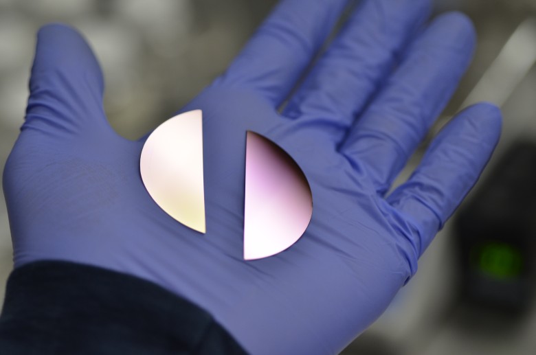 Oxidized plate
The oxidized plate is ready to form a pattern on the active / alloyed (P-type) area.
AZ4210 photoresist is applied on a
bench, rotating at about 3000 rpm, forming a film about 3.5 microns thick, which is dried carefully at 90 ° C on a hot plate.
Process lithography in detailThe mask of the active zone processes my
photolithographic Mark IV stepper in the ultraviolet at 365 nm steps - and the structure is processed in a solution of potassium hydroxide.
 Resist structure
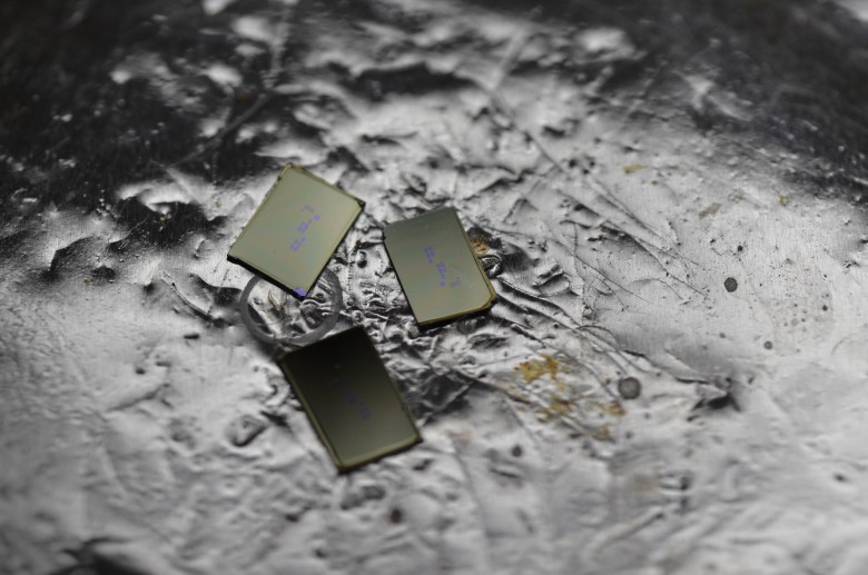 Resist structure
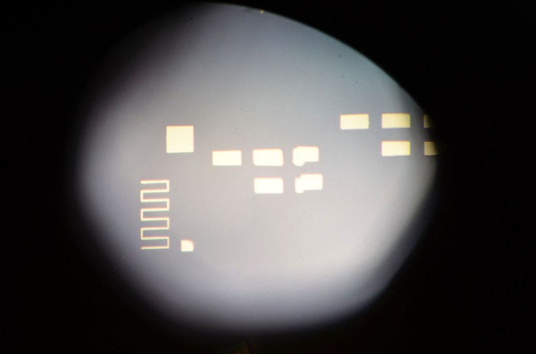 30 minute dry
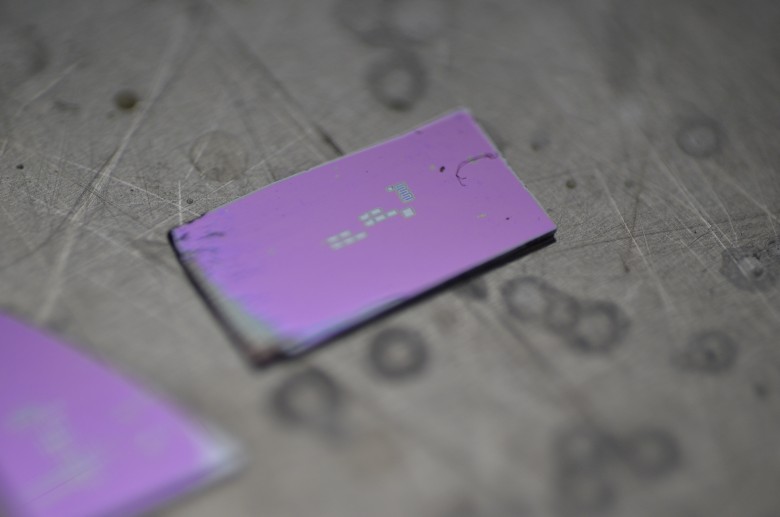 Core etching
After that, the resist structure is solidly hardened and
several other tricks are applied to ensure good adhesion and chemical resistance during the next etching in hydrogen fluoride, which transfers this structure to the gate oxide layer and opens the windows to bare silicon for doping. These regions will later become the source and drain of the transistor.
 Particles close the shutter
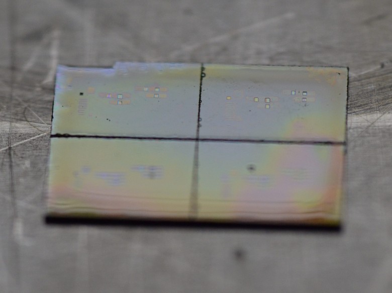 Etched crystals with etched closures
After this, doping is performed, that is, the introduction of impurities from a solid or liquid source. As a solid source, a disk of boron nitride is used, located nearby (less than 2 mm) from the plate in a tube furnace. Alternatively, it is possible to prepare a liquid source of phosphoric or boric acid in water or a solvent - and carry out doping according to the standard process of
transferring / immersion in hydrogen fluoride / diffusion / removal of glaze .
The above patterning steps are then repeated twice for the gate oxide and contact layer. The gate oxide should be much thinner (less than ~ 750 Å) than the protective oxide, so the zones between the drain / source are etched away - and a thinner oxide is grown there. Then, since the entire plate was oxidized during the doping step, contact windows should be etched to establish contact of the metal layer with the source / drain doped zones.
Now all transistors are formed and ready for interconnects with output to the lead frame. A protective layer of aluminum (400–500 nm) is
sprayed or
thermally sprayed onto the wafer. An alternative would be a method of
explosive lithography (lift-off process), when a photoresist is first formed, and then metal is deposited.
 Sprayed metal
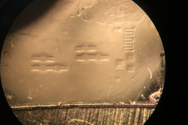 Sprayed metal
Then, a photolithography pattern is formed on the metal layer and etching in hot phosphoric acid occurs to complete the manufacture of the integrated circuit. The final steps before testing are visual inspection and high-temperature annealing of aluminum to form ohmic transitions.
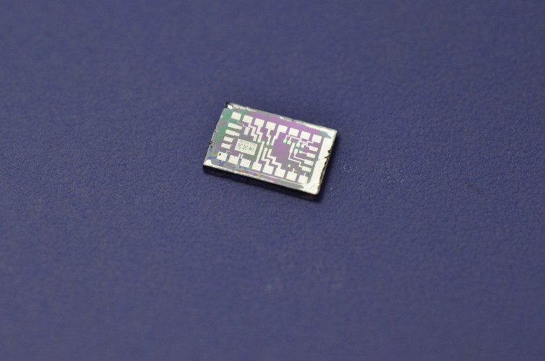
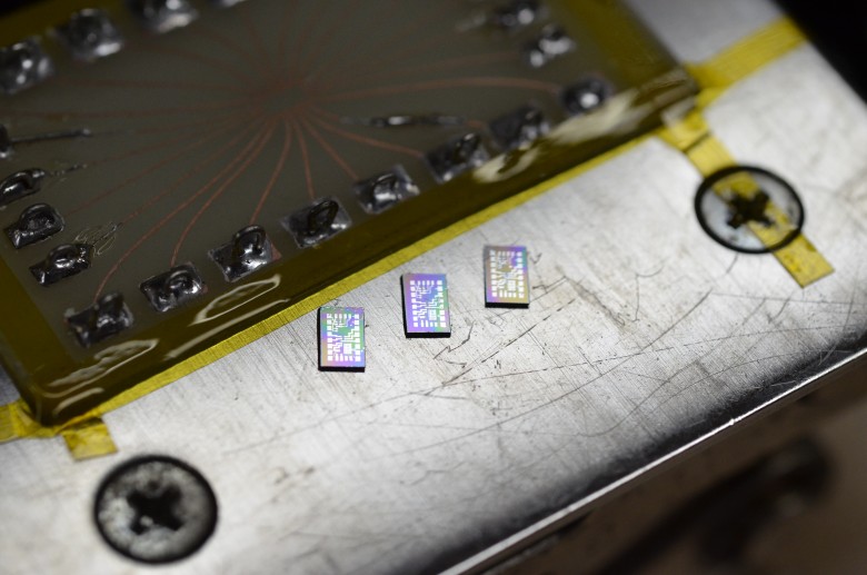
The microcircuit is now ready for packaging and testing.
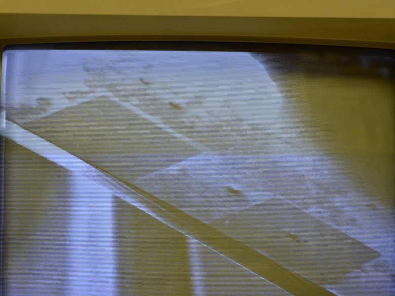
I do not have a micro-welding installation (I accept donations!), So now the testing process is limited to probing the plate with sharp tweezers or using a flip-chip board (difficult to level) with connection to a characterograph. The differential amplifier is also empirically tested in a circuit for operability testing.
 Curve IV
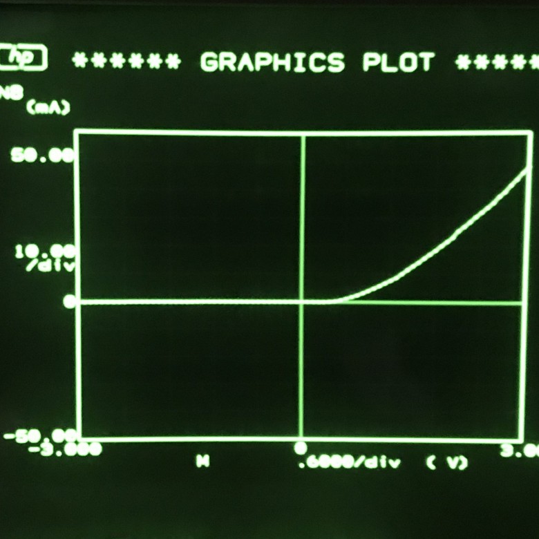 Curve IVFET Ids / Vds curve from previous NMOS device
Of course, these curves are far from ideal (including due to excessive contact resistance and other similar factors), but I expect improved performance if I get the installation of micro-welding. This may partly explain some of the differences from crystal to crystal. Soon I will add to
this page new IV curves, characteristics of a transistor and a differential amplifier.