World, PCB trace, May. Because PCB tracing is a labor. And this article opens a whole block, the purpose of which is to give the right tools for this task. It justifies the importance of monitoring the return current path and minimizing the inductance of the current circuit of critical signal lines, and also gives recommendations on their optimal tracing.
As already mentioned in the previous articles of the cycle, in the process of developing a printed circuit board, the possibilities of affordable technology for its production should be taken into account. At the same time, “accessibility” here should be understood as “accessibility within a given time, financial and organizational framework”. Technological constraints are particularly important at the PCB trace stage. Therefore, before starting the trace, it is recommended to study the technological standards of the intended manufacturer and create a set of rules in your CAD system that will be automatically monitored when tracing the printed circuit board. We will immediately stipulate that although modern CAD systems offer automatic tracers for printed circuit boards, they will not be discussed in this article and are not recommended for use in general. Only for a relatively simple project with a good placement of components and a well-thought-out set of rules, these tools make it possible to obtain a high-quality topology.
Do not forget about the return current
PCB tracing is a process in which the developer sets the paths for the currents to flow in the metallization layers of the printed circuit board. In electrical circuits, currents flow in closed paths - circuits - from the positive pole of the voltage source to the negative. Therefore, it is necessary to understand that the direct current flowing from the voltage source to the load always corresponds to the return current flowing from the load back to the source. This pair of currents forms a closed loop, the control of the parameters of which, especially in the case of high-frequency signals, is the main task of the developer. A large number of errors and problems with EMC and EMR of printed circuit boards is due to the fact that the developer does not analyze the trajectory and mutual influence of the return currents. In fig. Figure 1 shows the typical flow path of the signal line, and the colored rectangle highlights the area of this loop, which usually receives most of the developer’s attention, while the rest of the loop sometimes remains left to itself. The figure also reflects the fact that integrated circuits are not sources of electrical energy. They perform the function of complex key elements, while the sources of energy are batteries, capacitors of the power subsystem, and also sources external to the printed circuit board.

When the trajectory of the return current is not set by the developer, it is determined by the topology of the board (primarily the common wire) and the laws of physics (as always, by the way) —the current density distribution along the trajectories inversely related to their impedance. In the general case, this distribution is not analytically expressed, but for simple cases, solutions exist. In the
second article of the cycle, a recommendation was made to locate the signal layers near a continuous layer of earth or food. In this configuration, the distribution of the return current in the reference layer for the low-frequency signal is close to uniform (Fig. 2A), since as the current flow expands, the impedance determined by the resistive component decreases. With increasing frequency, the influence of the reactive component becomes decisive and the trajectory passing under the signal path has the minimum inductance, since the loop area is minimal (Fig. 2B, see
first article). The analytical formula for the distribution of the return current thin (width w ≤ h) of the microstrip line is given by the following formula (x is the distance from the geometric center of the line, h is the height above the reference layer):
This distribution provides the minimum inductance, that is, for all frequencies for which the ohmic resistance is negligible compared to the reactive one, it will be described by this formula. Distribution analysis shows that 50% of the current is concentrated in the ± h band, and 80% of the current in the ± 3h band.
It is important to understand that real signals consist of a set of frequencies that have a certain spectral distribution, while they often have a noise part, the spectrum of which can differ significantly from the spectrum of the signal itself. For example, in a “low-frequency” power line, significant high-frequency impulse noise may occur when switching digital circuits. Thus, for low-frequency components of the signal, the return current is distributed evenly in a wide region along the shortest path, and for high-frequency (f≳100 kHz) it is concentrated in a narrow region in the maximum proximity to the direct current.
Avoid cuts in the support layer
Any deviation in the current distribution from the optimum leads to an increase in the inductance of the current loop. Deviation occurs in the case of the presence of cuts (eng. Split, slot, gap) in the supporting layer, the cause of which can be through mechanical and vias, a number of vias or connector pins, a signal path in the supporting layer (Fig. 3). Howard Johnson in [2, section 5.3] gives an estimate of the inductance introduced by a narrow discontinuity of length D:
where w is the width of the path, the influence of the width of the gap itself is small. For a signal track with a width w = 0.2 mm at a break of length D = 1 cm, the increase in inductance will be ∆L1 ≈ 8 nH. For comparison, if the signal path were drawn around the gap, then its length would increase on average by D, which in turn, when the track height above the supporting layer h = 0.25 mm, would lead to a doubly increase in inductance:
Minimize inductance
Each element of the printed circuit board has a parasitic inductance - tracks, vias, solid layers, soldered joints, microcircuit pins, microwire unwinding. Why is it important to minimize the parasitic inductance of critical (aggressive sources of high-frequency noise and sensitive low-current analog circuits) lines? It is enough to recall several formulas into which the inductance enters as a parameter: a formula connecting the flux of a magnetic field and the strength of a current in a conductor
the formula connecting the induced emf when changing the current in the conductor
resonance frequency formulas
and good quality LC-circuit
Thus, the higher the inductance, the higher the radiation, the higher the impulse noise, including crosstalk, the lower the excitation frequency of parasitic oscillations and the longer their decay time. All these effects, of course, are undesirable, and the problems associated with them are far from always resolved by modifications to the printed circuit board, such as installing additional filtering components, shielding.
R.1.
It is critical to wiring high-frequency signal lines, minimizing the loop inductance, which is achieved by:
- minimizing the length of the printed track,
- exclusion of transitions between signal layers,
- close location of the track to the support layer,
- no gaps in the backing layer in the path of the return current.
If it is not possible to eliminate a lengthy gap in the support layer under the signal line, it is recommended to place at least one ceramic capacitor (English stitching capacitor) in maximum proximity to the signal line, providing a return current path through the cut. However, with an increase in the frequency of parasitic inductance of the capacitor and its compounds with the supporting layer, the efficiency of the solution decreases.
Optimize transitions between layers.
Separate consideration requires an important question of the transition of the track between the signal layers, because it is not always possible to eliminate cross lines for all critical signals. In fig. 4 shows the paths of direct and return currents for the various transition options between layers. The figure conventionally shows the effect of the skin effect: the return currents flow in the surface layer of the conductor. By increasing the number of red arrows, one can judge about the increase in the total inductance of the path to which the inductance of vias is added, and in the case of differing support layers, the inductance of the solder joints and the successive inductance of the capacitor (Eng. Equivalent series inductance, ESL). In addition, in the case of support layers of different potential, the high-frequency part of the return current flows in the form of bias currents (red dotted arrows). In addition to problems with the integrity of the signal, this leads to noise in this power supply circuit and an increase in the EMP level [3].
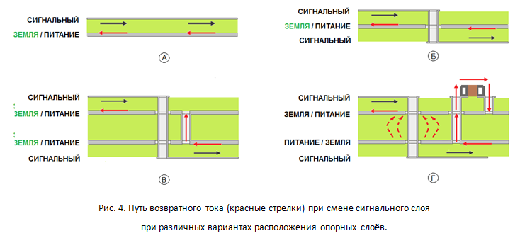
Henry Ott in [4, Section 16.3.3] cites experimental data, which investigated the change in the EMP level for a four-layer printed circuit board in the case of a transition of one high-frequency line from the upper layer to the lower one with the ground reference ones. The supporting layers were not interconnected by a via, but only due to capacitive coupling. The radiation level for the same board, where the signal line was diluted in one layer, was taken as the initial one. The increase was about 30 dB at a frequency of ~ 250 MHz, and only after 2 GHz the distributed capacity of the printed circuit board ensured a sufficiently low transition impedance between the supporting layers so that the EMR level differed little. The experiment shows the importance of eliminating transitions between signal layers for high-frequency lines.
R.2.
In cases where transition cannot be avoided, the following options are recommended in order of priority:
- between two layers adjacent to the same support layer (Fig. 4B),
- between two layers adjacent to the supporting layers of the same potential (power / ground), while in the maximum proximity to the place where the layer is changed (Fig. 4B) and, preferably, along the signal line, the supporting layers are connected by vias,
- between two layers adjacent to adjacent supporting layers of different potential, while in the maximum proximity to the place of layer change the supporting layers are connected by at least two ceramic capacitors with low inductance of the connection (Fig. 4D),
- between two layers adjacent to the spaced support layers of different potential, while in the maximum proximity to the place of layer change the support layers are connected by ceramic capacitors with low connection inductance — not recommended for critical signals with fronts of the order of 1 ns.
Switching between more than two layers for critical signals is not recommended. The preferred support layer in the first two variants is the ground layer. If the base layer is the power layer, then it is necessary to ensure low impedance of the power subsystem in the signal spectrum band. Note that most often there is a sufficiently large number of ceramic capacitors near the microcircuit, so changing the layer by the signal path near the receiver / transmitter is the most optimal and, at best, will not require the placement of additional components.
In complex printed circuit boards, there are many signal lines and it is not possible to implement the recommendations given in this article for all signals, especially given the high demands on the dimensions of the final products. That is why it is necessary to single out a group of critical high-frequency and sensitive signals and start tracing from them. At the same time, the location of the components associated with this group should ensure the optimal wiring of critical signals. The task of minimizing the inductance of the current loop is only one of the aspects of the tracing of signal lines. In the next articles of the cycle, wiring techniques and matching schemes that reduce reflections and crosstalk in the lines will be considered.
Literature
[1] Holloway CL, Kioster EF "Microstrip Line Closed-Form", with Applications to the Ground Plane Loss. IEEE Transactions on Theory and Techniques, vol. 43, no. 5, May 1995.
[2] Johnson H. "High Speed Digital Design: A Handbook of Black Magic", Prentice Hall, 1993.
[3] Cui W., Ye X., Archambeault B., etc. “EMI Resulting from Signal Via Transitions through the DC Power Bus,” IEEE International Symposium on Electromagnetic Compatibility, 2000.
[4] Ott, HW Electromagnetic Compatibility Engineering, Wiley, 2009.
The article was first published in the journal "Components and Technologies" 2018, №2. The publication on “Geektimes” is coordinated with the editors of the magazine.