Translation by Ken Shirriff
Almost every smartphone uses a processor based on the ARM1 chip, introduced in 1985. More than ten billion ARM cores have been used in various gadgets, including one of Apple’s biggest failures, the Newton handheld computer, and one of its most deafening successes — the iPhone. In this article, we will look at the key parts of the ARM1 processor: describe the general structure of the chip, look at how transistors are designed and how they function, interacting with each other for storing and processing data, and also look at the
visual simulation of this microprocessor and find out what inside the ARM1 during its operation.
ARM1 chip overview
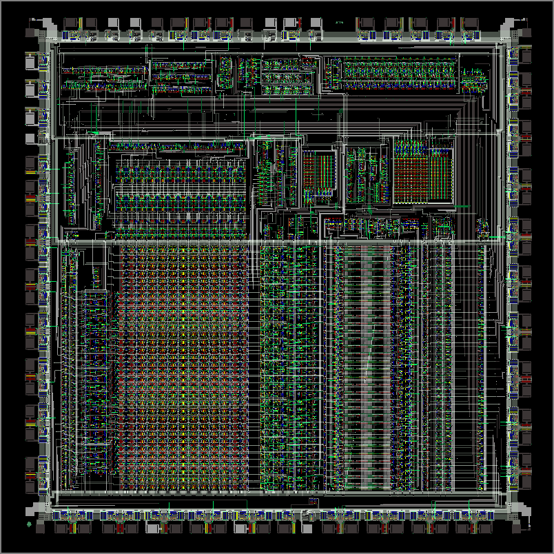
The ARM1 microprocessor is built from functional blocks, each of which has a specific purpose. Registers store data, ALU performs simple arithmetic, instruction decoders determine how to execute each instruction, and so on. Compared to most processors, the ARM1 chip layout is simple, and each functional block is well distinguished. For comparison, the layout of chips, such as the 6502 or Z-80, is manually optimized to avoid empty spaces on the substrate. In these processors, functional blocks are glued together, which complicates their understanding.
 The main components of the ARM1 chip. Unmarked contacts are different control signals.
Now you see an image showing the most important functional parts of the ARM microprocessor. The actual processing takes place at the bottom of the chip, which refers to the data path. The chip processes 32 bits simultaneously, therefore its structure includes 32 horizontal layers: 31 bits from above, 0 bits from below. Several data buses operate horizontally to interconnect various chip components. On the image you can see a large section of twenty-five registers. The command counter (the fifteenth register) is to the left of the register section, and the zero register is to the right. Nine of the twenty-five registers are optional, since there are copies of some registers for use in interrupt handling.
All calculations occur in the arithmetic logic unit (ALU), which is located to the right of the block of registers. The ALU performs 16 different operations: addition, addition with transfer, subtraction, logical addition, and so on ... The ALU uses two 32-bit inputs and outputs 32 bits at the output. More information about the device ALU can be found
here . To the right of the ALU is a 32-bit shifter. This large component performs a binary input cyclic shift operation. On the left are the address lines that provide access to the addresses in the memory via address contacts. On the right are the data lines that read and write data values to the memory.
On top is the control unit. The control lines are drawn vertically from the control unit to the data line diagram below. These signals select registers, tell the ALU what operation to perform, and so on. The command decode circuitry processes each instruction and generates the necessary control signals. The register decoding unit processes the register selection bits in an instruction and generates control signals to select the necessary registers.
Contacts
The squares around the outer surface of the image are the pads that connect the processor to the outside world. The photo below shows the eighty-four-pin ARM1 microprocessor housing. Gold-plated contacts are connected to pads on a silicon chip inside the case.
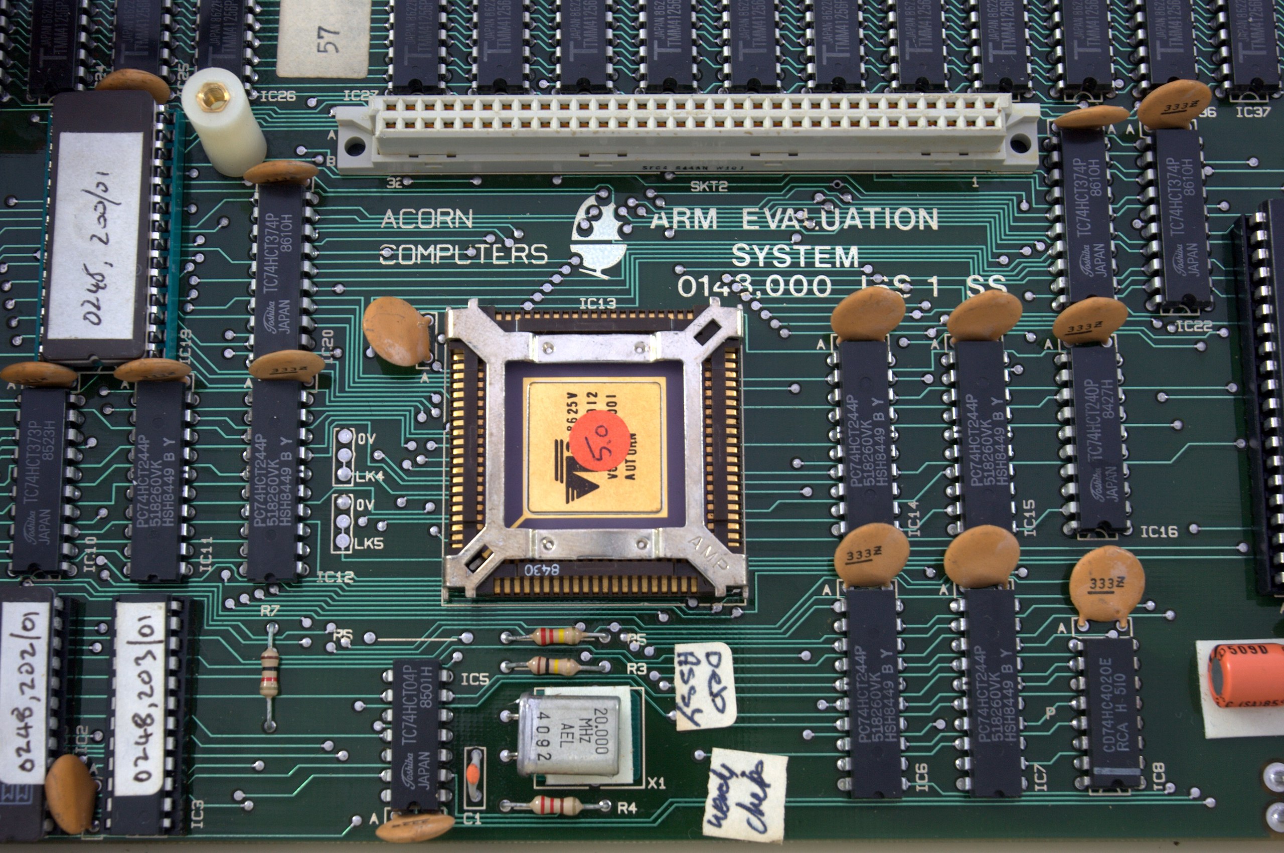 ARM1 processor installed in Acorn ARM Evaluation System
Most sites are used for address lines and data leading to memory. The chip has 26 address lines that allow it to access 64 MB of memory and 32 data lines, allowing it to read or write 32 bits at a time. The address lines are in the lower left corner, and the data lines are in the right. In the simulation model of the chip, you can see that the signals arrive at the lines of the memory address, and the data lines read information from the memory. The right side of the simulator shows the address and data values in hexadecimal format. If you know the hexadecimal number system, you can easily match these values with the contact states.
Each corner of the chip has a power line (+) and a ground line (-), providing a supply voltage of 5 volts, which is necessary for the operation of the chip. Various control signals are located at the top of the chip. In the simulator, it is easy to notice two clocks that set a clock pulse. The frequencies of phase 1 and phase 2 alternate, providing the clock signal necessary for the operation of the chip. In our visual simulation, it becomes active about twice per second, but the real chip has a frequency of 8 megahertz, which is more than a million times faster. Pay attention to the manufacturer's name "ACORN" on the chip instead of 82 contacts.
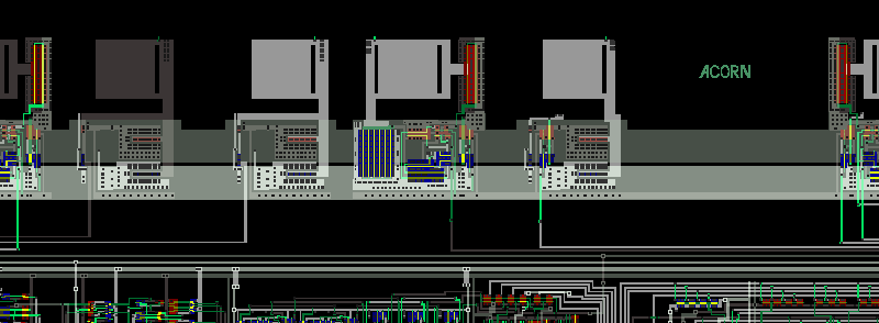 Two clocking signals
ARM processor history
The ARM1 microprocessor was designed in 1985 by engineers Sophie Wilson and Steve Farber of Acorn Computers. Initially, the chip was called Acorn RISC Machine and was intended as a coprocessor for the
BBC Micro computer.
 Sophie Wilson and Steve Farber
A total of several hundred ARM1 microprocessors were produced, so you might think that it was lost in the depths of the microprocessor history of the 1980s. However, the first ARM1 chip led to a surprisingly successful ARM architecture, with more than 50 billion units in chips. What happened?
In the early 1980s, research suggested that if you simplify the set of instructions for the processor, developers will get better performance - the processor will be simple, but faster: a computer with a reduced instruction set or RISC (reduced instruction set computer).
Stanford and
Berkeley 's research work inspired ARM developers to choose RISC architecture. In addition, given the small Acorn development team, the choice of RISC was a practical solution.
On a computer with the RISC architecture, the instruction set was limited to the most frequently used ones, optimized for high performance and executed per cycle. The instructions in turn are a fixed size that simplifies the logic for decoding instructions. The RISC processor requires far fewer circuits to control and decode instructions, which allows more components to be placed on the chip.
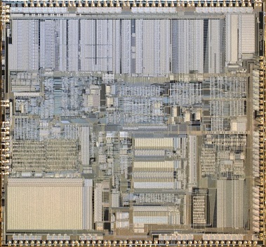
The simplicity of the RISC design is evident when comparing microprocessors ARM1 and Intel 80386, released in the same year: ARM1 had about twenty-five thousand transistors, and 80386 - two hundred and seventy-five thousand. Below are two photos of processors at the same scale. The area of the ARM1 crystal is fifty square millimeters, compared to one hundred and four square millimeters for the 386th.

Due to the small number of transistors, the ARM1 processor had a small power: about one tenth of a watt compared to almost two watts of the 386th. The combination of high performance and low power consumption made later versions of ARM microprocessors very popular for embedded systems. Apple has selected an ARM processor for its ill-fated Newton pocket system. In 1990, Acorn Computers, Apple and chipmaker VLSI Technology formed Advanced RISC Machines to continue the development of ARM.
Since then, ARM has become the most popular architecture with more than fifty billion processors. Most mobile devices use an ARM microprocessor. For example, the Apple A8 processor inside the iPhone 6 uses 64-bit ARMv8-A. Despite its modest beginnings, ARM1 was on the IEEE Spectrum list
of 25 chips that shook the world and became the most influential microprocessor PC World ever.
Interestingly, ARM does not produce chips. Instead, ARM's intellectual property is licensed to hundreds of different companies that produce chips using the ARM architecture.
Low level chip structure
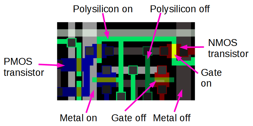
The microprocessor ARM1 consists of five layers. If you increase the scale of the chip in the simulation model, you can see the components of the chip, built from these layers. The simulation model uses a specific color for each layer and denotes activity lines in its own color. The bottom layer consists of silicon, on which transistors are located. During production, areas of silicon are modified (doped) with the use of various impurities. Silicon can be doped positively to form a P-MOS transistor (blue) or negative for an N-MOS transistor (red). Unalloyed silicon is mainly an insulator (black).
 ARM1 simulator presents different layers with its colors
Polysilicon lines marked in green are applied over silicon. When polysilicon crosses doped silicon, it forms the gate of the transistor (yellow). Finally, two metal layers, marked in gray, are located on top of polysilicon and provide conductivity. Black squares are contacts that form connections between different layers.
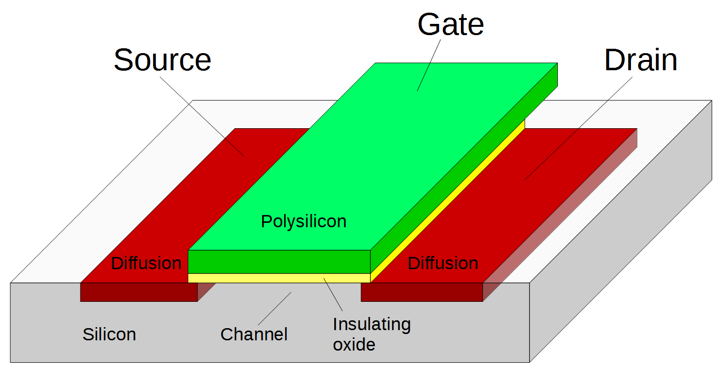
For our purposes, the MOSFET can be considered as a switch controlled by the gate. When it is turned on (closed), the drain and source in the silicon regions are connected. When it is disabled (open) the drain and source are disconnected.
 MOSFET Structure
Like most modern processors, ARM1 was built using CMOS technology, which uses two types of MOS transistors: N-channel and P-channel. N-channel MOS transistors are turned on only when a high level signal is applied to the gate and the output is extended to ground. P-channel MOS transistors are turned on when the gate signal is low and the output voltage is five volts.
Register File Concept
The register file is a key component of the ARM1, which stores information inside the chip. The register file consists of twenty-five registers, each of which contains thirty-two bits.
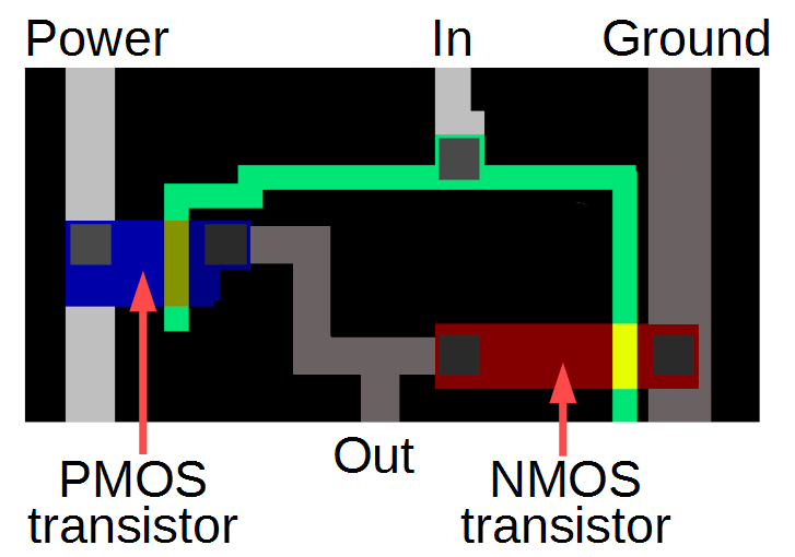
The image below shows the two transistors that make up the inverter. If a high level signal arrives, the N-MOS transistor (red) turns on, connecting the output to ground to provide a low level signal at the output. If the input signal is low, the transistor P-MOS (blue) is turned on, connecting the power line to the output, so that the output has a high level signal. Thus, the output is opposite to the input, creating an inverter.
 Inverter
The combination of two inverters in a loop form a simple storage scheme. If the output of the first inverter is 1, the second produces 0, which is fed to the input of the first inverter and 1 is created at its output - the circuit is stable. Accordingly, the circuit will remain in such a state indefinitely, “remembering” one bit until it is forcibly transferred to another state.
 Two inverters form a register that can store 1 bit
To create such a scheme in the register cell used, read and write lines are added, as well as lines of choice for connecting the cell to the bus lines. When the write line is activated, the bus is in contact with the inverter, allowing you to overwrite the current value with a new bit. Similarly, transistors connect a bit to the read bus when the corresponding selection line is activated, allowing you to read the stored value.
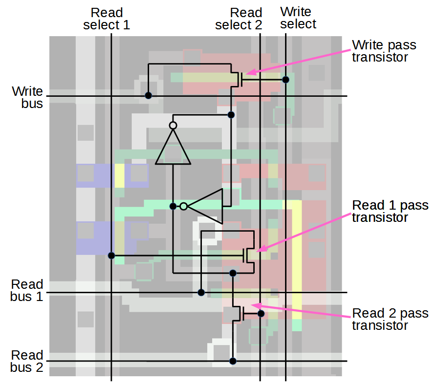 Scheme of one bit of the register file ARM1
To create a register file, the register cell must be repeated 32 times vertically for each bit, and 25 times horizontally to form each register. Each register has three horizontal lines — a recording line and two reading lines. Each register has three vertical control lines — a write selection line and two read selection lines. When activating the desired control lines, two registers can be read and one register can be written at a time. In the simulation model, you can see active vertical control lines for selecting registers and data bits moving along horizontal bus lines.
Looking at the memory cell in the simulator, you can determine which inverter is turned on and determine whether bit 0 or 1 is equal. If the top inverter input is active, then the bit is zero. If the input of the lower inverter is active, then the bit is equal to one. Thus, carefully looking at, you can read the values of the registers directly from the simulator.
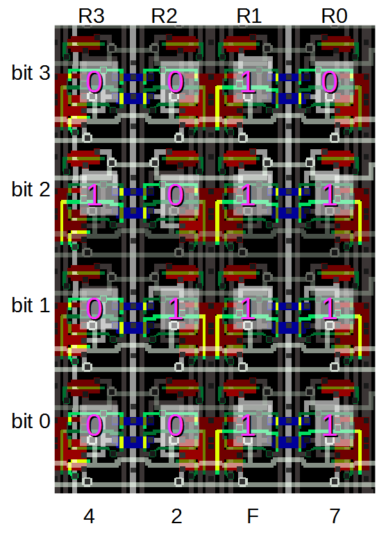 Image of the ARM1 register file
Quick shift device
The fast-shear device performs binary shifts and is another interesting component of the ARM1. Most instructions use a shifter that allows you to shift a binary argument to the right, left, or alternate any characters (from 0 to 31 bits). During the launch of the simulator, you can see diagonal lines moving to the right and left in a quick shift.
The image below shows the structure of the shear device. The bits are shifted vertically with respect to the zero and thirty-first bits. The output bits are shifted horizontally between the zero bit from the bottom and the thirty-first bit from the top. Diagonal lines indicate where the vertical lines are connected to the horizontal, generating a shift at the exit. Different positions of the diagonal line lead to different shifts. The upper diagonal line moves the bits to the left, and the lower diagonal line to the right. During the shift both diagonals are active; this may not be noticeable, but in the shift part of the word, the part shifts to the right, and often to the left.
 The structure of the rapid shift device
Let's zoom in on the shear device to get a better look at its main components. It contains 32 to 32 cross sections of transistors, each of which connects one vertical line with one horizontal. Transistor gates are connected by diagonal control lines; transistors along the active diagonal connect the corresponding vertical and horizontal lines. Thus, by activating the corresponding diagonals, the output lines are connected to the input lines shifted by a certain number of bits. Since the chip input lines function horizontally, there are 32 connections between the input lines and the corresponding vertical bit lines.
 Detailed consideration of the ARM1 rapid shear device
Conclusion
The ARM1 microprocessor has led to the amazingly successful ARM processor architecture, which is the heart of your smartphone and of any mobile device in general. The simple architecture of the RISC chip ARM1 simplifies the understanding of the microprocessor circuit as compared to the structure 80386. The fascinating visual simulation of the ARM microprocessor helps to understand what is happening inside it.
Our video created for this article:
Inside CPU: ARM1